SCAS984 March 2024 SN74AHCT595-Q1
PRODUCTION DATA
- 1
- 1 Features
- 2 Applications
- 3 Description
- 4 Pin Configuration and Functions
- 5 Specifications
- 6 Parameter Measurement Information
- 7 Detailed Description
- 8 Application and Implementation
- 9 Device and Documentation Support
- 10Revision History
- 11Mechanical, Packaging, and Orderable Information
Package Options
Refer to the PDF data sheet for device specific package drawings
Mechanical Data (Package|Pins)
- BQB|16
- PW|16
Thermal pad, mechanical data (Package|Pins)
- BQB|16
Orderable Information
3 Description
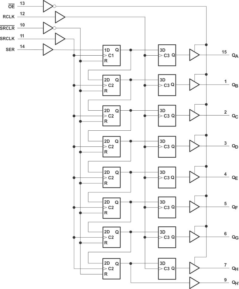
The SN74AHCT595-Q1 devices contain an 8-bit serial-in, parallel-out shift register that feeds an 8-bit D-type storage register. Both the shift register clock (SRCLK) and storage register clock (RCLK) are positive-edge triggered.
Package Information
| PART NUMBER | PACKAGE(1) | PACKAGE SIZE(2) | BODY SIZE (NOM)(3) |
|---|---|---|---|
| SN74AHCT595-Q1 | BQB (WQFN, 16) | 3.5mm × 2.5mm | 3.5mm × 2.5mm |
| PW (TSSOP, 16) | 5.0mm × 6.4mm | 5.0mm × 4.4mm |
(1) For more information, see Section 11.
(2) The package size (length × width)
is a nominal value and includes pins, where
applicable.
(3) The body size (length × width) is a
nominal value and does not include pins.

Pin
numbers shown are for the PW and BQB
packages.
Simplified
Schematic