SCAS416Q March 1994 – September 2016 SN74ALVC164245
PRODUCTION DATA.
- 1 Features
- 2 Applications
- 3 Description
- 4 Revision History
- 5 Pin Configuration and Functions
-
6 Specifications
- 6.1 Absolute Maximum Ratings
- 6.2 ESD Ratings
- 6.3 Recommended Operating Conditions: VCCB at 3.3 V
- 6.4 Recommended Operating Conditions: VCCA at 2.5 V
- 6.5 Thermal Information
- 6.6 Electrical Characteristics: VCCA = 2.7 V to 3.6 V
- 6.7 Electrical Characteristics: VCCA = 2.3 V to 2.7 V
- 6.8 Switching Characteristics
- 6.9 Operating Characteristics
- 6.10 Typical Characteristics
- 7 Parameter Measurement Information
- 8 Detailed Description
- 9 Application and Implementation
- 10Power Supply Recommendations
- 11Layout
- 12Device and Documentation Support
- 13Mechanical, Packaging, and Orderable Information
Package Options
Mechanical Data (Package|Pins)
Thermal pad, mechanical data (Package|Pins)
Orderable Information
8 Detailed Description
8.1 Overview
The SN74ALVC16245 device is designed for asynchronous communication between data buses. The control-function implementation minimizes external timing requirements.
This device can be used as two 8-bit transceivers or one 16-bit transceiver. It allows data transmission from the A bus to the B bus or from the B bus to the A bus, depending on the logic level at the direction-control (DIR) input. The output-enable (OE) input can be used to disable the device so that the buses are effectively isolated. To ensure the high-impedance state during power up or power down, OE should be tied to VCC through a pullup resistor; the minimum value of the resistor is determined by the current-sinking capability of the driver.
Inputs can be driven from either 3.3-V or 5-V devices. This feature allows the use of this device as a translator in a mixed 3.3-V and 5-V system environment.
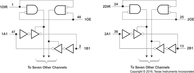
8.2 Functional Block Diagram
 Figure 6. Logic Diagram (Positive Logic)
8.3 Feature Description
The SN74ALVC164245 can output 24 mA drive at 3.3V VCC. This device allows down voltage translations and accepts input voltages to VCC + 0.5V. This device is useful for high-speed applications because of the low tpd.
8.4 Device Functional Modes
Table 3 lists the functions of the device.
Table 3. Function Table(1)
(Each 8-Bit Section)
| CONTROL INPUTS | OUTPUT CIRCUITS | OPERATION | ||
|---|---|---|---|---|
| OE | DIR | A PORT | B PORT | |
| L | L | Enabled | Hi-Z | B data to A bus |
| L | H | Hi-Z | Enabled | A data to B bus |
| H | X | Hi-Z | Hi-Z | Isolation |