SCAS416Q March 1994 – September 2016 SN74ALVC164245
PRODUCTION DATA.
- 1 Features
- 2 Applications
- 3 Description
- 4 Revision History
- 5 Pin Configuration and Functions
-
6 Specifications
- 6.1 Absolute Maximum Ratings
- 6.2 ESD Ratings
- 6.3 Recommended Operating Conditions: VCCB at 3.3 V
- 6.4 Recommended Operating Conditions: VCCA at 2.5 V
- 6.5 Thermal Information
- 6.6 Electrical Characteristics: VCCA = 2.7 V to 3.6 V
- 6.7 Electrical Characteristics: VCCA = 2.3 V to 2.7 V
- 6.8 Switching Characteristics
- 6.9 Operating Characteristics
- 6.10 Typical Characteristics
- 7 Parameter Measurement Information
- 8 Detailed Description
- 9 Application and Implementation
- 10Power Supply Recommendations
- 11Layout
- 12Device and Documentation Support
- 13Mechanical, Packaging, and Orderable Information
Package Options
Mechanical Data (Package|Pins)
Thermal pad, mechanical data (Package|Pins)
Orderable Information
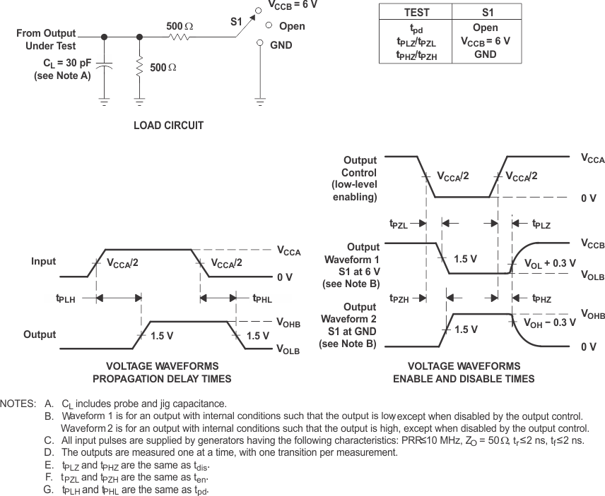
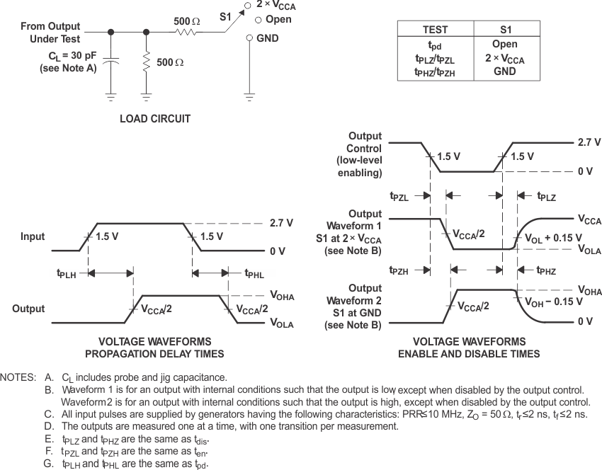
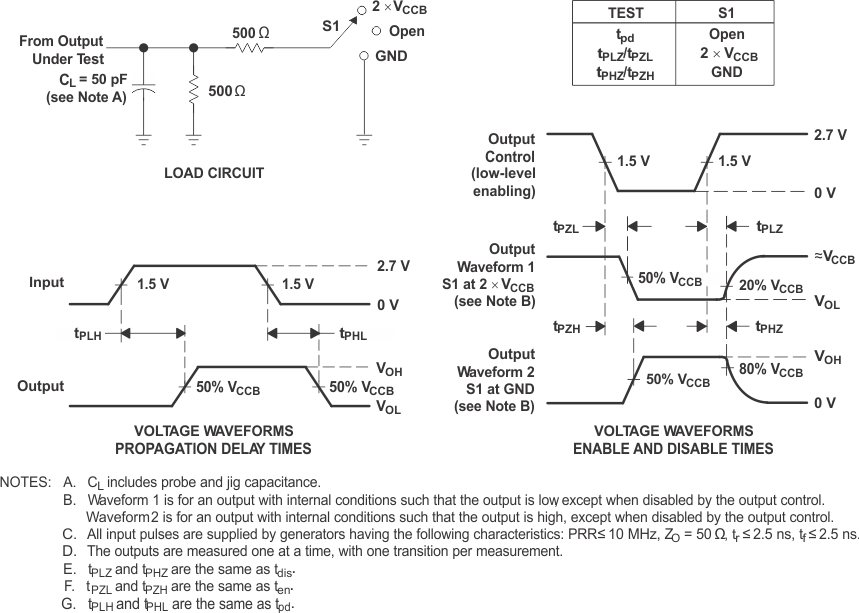
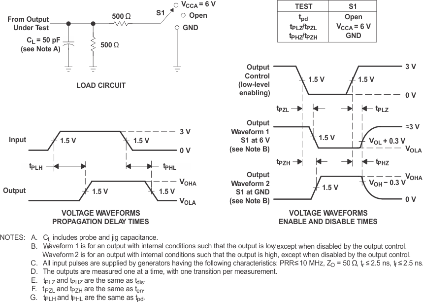
7 Parameter Measurement Information
7.1 VCCA = 2.5 V ± 0.2 V to VCCB = 3.3 V ± 0.3 V
 Figure 2. Load Circuit and Voltage Waveforms
7.2 VCCB = 3.3 V ± 0.3 V to VCCA = 2.5 V ± 0.2 V
 Figure 3. Load Circuit and Voltage Waveforms
7.3 VCCA = 3.3 V ± 0.3 V to VCCB = 5 V ± 0.5 V
 Figure 4. Load Circuit and Voltage Waveforms
7.4 VCCB = 5 V ± 0.5 V to VCCA = 2.7 V and 3.3 V ± 0.3 V
 Figure 5. Load Circuit and Voltage Waveforms