-
SN74AUC1G126 Single Bus Buffer Gate With Tri-state Output
- 1 Features
- 2 Applications
- 3 Description
- 4 Revision History
- 5 Pin Configuration and Functions
- 6 Specifications
- 7 Typical Characteristics
- 8 Parameter Measurement Information
- 9 Detailed Description
- 10Application and Implementation
- 11Power Supply Recommendations
- 12Layout
- 13Device and Documentation Support
- 14Mechanical, Packaging, and Orderable Information
- IMPORTANT NOTICE
Package Options
Refer to the PDF data sheet for device specific package drawings
Mechanical Data (Package|Pins)
- DBV|5
- DCK|5
- YZP|5
Thermal pad, mechanical data (Package|Pins)
Orderable Information
SN74AUC1G126 Single Bus Buffer Gate With Tri-state Output
1 Features
- Latch-Up Performance Exceeds 100 mA Per JESD 78, Class II
- ESD Protection Exceeds JESD22
- 2000-V Human-Body Model (A114-A)
- 200-V Machine Model (A115-A)
- 1000-V Charged-Device Model (C101)
- Available in TI's NanoFree™ Package
- Optimized for 1.8-V Operation and is 3.6-V I/O Tolerant to Support Mixed-Mode Signal Operation
- Ioff Supports Partial Power Down Mode and Back Drive Protection
- Sub-1 V Operable
- Maximum tpd of 2.5 ns at 1.8 V
- Low Power Consumption, 10-µA Maximum ICC
- ±8-mA Output Drive at 1.8 V
2 Applications
- AV Receiver
- Audio Dock: Portable
- Blu-ray™ Player and Home Theater
- Embedded PC
- MP3 Player/Recorder (Portable Audio)
- Personal Digital Assistant (PDA)
- Power: AC/DC Supply, Single Controller
- Solid State Drive (SSD): Client and Enterprise
- TV: LCD, Digital, and High-Definition (HD)
- Tablet: Enterprise
- Video Analytics: Server
- Wireless Headset, Keyboard, and Mouse
3 Description
The SN74AUC1G126 bus buffer gate is operational at 0.8-V to 2.7-V VCC, but is designed specifically for 1.65-V to 1.95-V VCC operation.
The SN74AUC1G126 device is a single line driver with a tri-state output. The output is disabled when the output-enable (OE) input is low.
To ensure the high-impedance state during power up or power down, OE should be tied to GND through a pulldown resistor; the minimum value of the resistor is determined by the current-sourcing capability of the driver.
NanoFree™ package technology is a major breakthrough in device packaging concepts, using the die as the package.
This device is fully specified for partial-power-down applications using Ioff. The Ioff circuitry disables the outputs, which prevents damaging current backflow through the device when it is powered down.
Device Information(1)
| PART NUMBER | PACKAGE | BODY SIZE (NOM) |
|---|---|---|
| SN74AUC1G126DBV | SOT-23 (5) | 2.90 mm × 1.60 mm |
| SN74AUC1G126DCK | SC70 (5) | 2.00 mm × 1.25 mm |
| SN74AUC1G126YZP | DSBGA (5) | 1.388 mm × 0.888 mm |
- For all available packages, see the orderable addendum at the end of the data sheet.
Device Images
Logic Diagram (Positive Logic)

4 Revision History
Changes from K Revision (June 2017) to L Revision
- Updated body size of YZP package. Go
- Added junction temperature to Absolute Maximum RatingsGo
- Add Detailed Description, Application and Implementation, Power Supply Recommendations, and Layout sectionsGo
Changes from J Revision (July 2007) to K Revision
- Deleted DRY package throughout data sheetGo
- Added Applications, Device Information table, ESD Ratings table, Thermal Information table, Feature Description section, Device Functional Modes, Device and Documentation Support section, and Mechanical, Packaging, and Orderable Information sectionGo
- Deleted Ordering Information table, see Mechanical, Packaging, and Orderable Information at the end of the data sheet Go
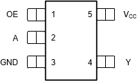
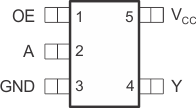
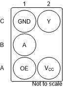
5 Pin Configuration and Functions


Pin Functions
| PIN | I/O | DESCRIPTION | ||
|---|---|---|---|---|
| NAME | DBV, DCK | YZP | ||
| A | 2 | B1 | I | Logic input |
| GND | 3 | C1 | — | Ground |
| OE | 1 | A1 | I | Output enable |
| VCC | 5 | A2 | — | Positive supply |
| Y | 4 | C2 | O | Output |