SCES387L march   2002  – June 2017 SN74AUC1G79

UNLESS OTHERWISE NOTED, this document contains PRODUCTION DATA.  

  1. Features
  2. Applications
  3. Description
  4. Revision History
  5. Pin Configuration and Functions
  6. Specifications
    1. 6.1 Absolute Maximum Ratings
    2. 6.2 ESD Ratings
    3. 6.3 Recommended Operating Conditions
    4. 6.4 Thermal Information
    5. 6.5 Electrical Characteristics
    6. 6.6 Timing Requirements
    7. 6.7 Switching Characteristics: CL = 15 pF
    8. 6.8 Switching Characteristics: CL = 30 pF
    9. 6.9 Operating Characteristics
  7. Parameter Measurement Information
  8. Detailed Description
    1. 8.1 Functional Block Diagram
    2. 8.2 Device Functional Modes
  9. Device and Documentation Support
    1. 9.1 Documentation Support
      1. 9.1.1 Related Documentation
    2. 9.2 Receiving Notification of Documentation Updates
    3. 9.3 Community Resources
    4. 9.4 Trademarks
    5. 9.5 Electrostatic Discharge Caution
    6. 9.6 Glossary
  10. 10Mechanical, Packaging, and Orderable Information

Package Options

Refer to the PDF data sheet for device specific package drawings

Mechanical Data (Package|Pins)
  • DBV|5
  • DCK|5
Thermal pad, mechanical data (Package|Pins)
Orderable Information

Pin Configuration and Functions

DBV Package
5-Pin SOT-23
Top View
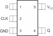
SN74AUC1G79 po2_ces387-1.gif
DCK Package
5-Pin SC70
Top View
SN74AUC1G79 po2_ces387-2.gif
YZP Package
5-Pin DSBGA
Bottom View
SN74AUC1G79 SN74AUC1G79_yzp_po.gif
See mechanical drawings for dimensions.

Pin Functions

PIN I/O DESCRIPTION
NAME DBV, DCK YZP
CLK 2 B1 I Clock input
D 1 A1 I Data input
GND 3 C1 Ground
Q 4 C2 O Latched output
VCC 5 A2 Positive supply