SCES681E January 2008 – April 2024 SN74AUP2G08
PRODUCTION DATA
- 1
- 1 Features
- 2 Applications
- 3 Description
- 4 Pin Configuration and Functions
-
5 Specifications
- 5.1 Absolute Maximum Ratings
- 5.2 ESD Ratings
- 5.3 Recommended Operating Conditions
- 5.4 Thermal Resistance Characteristics
- 5.5 Electrical Characteristics
- 5.6 Switching Characteristics - CL = 5 pF
- 5.7 Switching Characteristics - CL = 10 pF
- 5.8 Switching Characteristics - CL = 15 pF
- 5.9 Switching Characteristics - CL = 30 pF
- 5.10 Operating Characteristics
- 5.11 Typical Characteristics
- 6 Parameter Measurement Information
- 7 Detailed Description
- 8 Application and Implementation
- 9 Device and Documentation Support
- 10Revision History
- 11Mechanical, Packaging, and Orderable Information
Package Options
Mechanical Data (Package|Pins)
Thermal pad, mechanical data (Package|Pins)
Orderable Information
3 Description
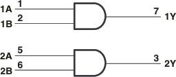
This dual 2-input positive-AND gate is designed for 0.8V to 3.6V VCC operation and performs the Boolean function Y = A ● B in positive logic.
This device is fully specified for partial-power-down applications using Ioff. The Ioff circuitry disables the outputs when VCC = 0V, preventing damaging current backflow through the device when it is powered down.
Package Information
| PART NUMBER | PACKAGE(1) | PACKAGE SIZE(2) | BODY SIZE (NOM)(3) |
|---|---|---|---|
|
SN74AUP2G08 |
DCU (VSSOP, 8) | 3.1mm × 2mm | 2.3mm × 2mm |
| DQE (X2SON, 8) | 1mm × 1.4mm | 1mm × 1.4mm | |
| RSE (UQFN, 8) | 1.5mm × 1.5mm | 1.5mm × 1.5mm | |
| YFP (DSBGA, 8) | 0.76mm × 1.56mm | 0.76mm × 1.56mm | |
| YZP (DSBGA, 8) | 0.89mm × 1.89mm | 0.89mm × 1.89mm |
(1) For more information, see Section 11.
(2) The package size (length × width) is a nominal value and includes pins, where applicable.
(3) The body size (length × width) is a nominal value and does not include pins.
 Simplified Logic Diagram (Positive Logic)