SCES971 May 2024 SN74AVC1T45-Q1
PRODUCTION DATA
- 1
- 1 Features
- 2 Applications
- 3 Description
- 4 Pin Configuration and Functions
-
5 Specifications
- 5.1 Absolute Maximum Ratings
- 5.2 ESD Ratings
- 5.3 Recommended Operating Conditions
- 5.4 Thermal Information
- 5.5 Electrical Characteristics
- 5.6 Switching Characteristics, VCCA = 1.2 ± 0.12V
- 5.7 Switching Characteristics, VCCA = 1.5 ± 0.1V
- 5.8 Switching Characteristics, VCCA = 1.8 ± 0.15V
- 5.9 Switching Characteristics, VCCA = 2.5 ± 0.2V
- 5.10 Switching Characteristics, VCCA = 3.3 ± 0.3V
- 5.11 Operating Characteristics
- 5.12 Typical Characteristics
- 6 Parameter Measurement Information
- 7 Detailed Description
- 8 Application and Implementation
- 9 Device and Documentation Support
- 10Revision History
- 11Mechanical, Packaging, and Orderable Information
Package Options
Refer to the PDF data sheet for device specific package drawings
Mechanical Data (Package|Pins)
- DCK|6
Thermal pad, mechanical data (Package|Pins)
Orderable Information
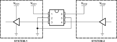
8.2.1 Unidirectional Logic Level-Shifting Application
Figure 8-1 shows an example of the SN74AVC1T45-Q1 being used in a unidirectional logic level-shifting application.
 Figure 8-1 Unidirectional Logic Level-Shifting Application
| PIN | NAME | FUNCTION | DESCRIPTION |
|---|---|---|---|
| 1 | VCCA | VCC1 | SYSTEM-1 supply voltage (1.2V to 3.6V) |
| 2 | GND | GND | Device GND |
| 3 | A | OUT | Output level depends on VCC1 voltage. |
| 4 | B | IN | Input threshold value depends on VCC2 voltage. |
| 5 | DIR | DIR | GND (low level) determines B-port to A-port direction. |
| 6 | VCCB | VCC2 | SYSTEM-2 supply voltage (1.2V to 3.6V) |