SCES531M December 2003 – October 2024 SN74AVC2T45
PRODUCTION DATA
- 1
- 1 Features
- 2 Applications
- 3 Description
- 4 Pin Configuration and Functions
-
5 Specifications
- 5.1 Absolute Maximum Ratings
- 5.2 ESD Ratings
- 5.3 Recommended Operating Conditions
- 5.4 Thermal Information
- 5.5 Electrical Characteristics
- 5.6 Switching Characteristics: VCCA = 1.2 V
- 5.7 Switching Characteristics: VCCA = 1.5 V ±0.1 V
- 5.8 Switching Characteristics: VCCA = 1.8 V ±0.15 V
- 5.9 Switching Characteristics: VCCA = 2.5 V ±0.2 V
- 5.10 Switching Characteristics: VCCA = 3.3 V ±0.3 V
- 5.11 Operating Characteristics
- 5.12
Typical Characteristics
- 5.12.1 Typical Propagation Delay (A to B) vs Load Capacitance, TA = 25°C, VCCA = 1.2 V
- 5.12.2 Typical Propagation Delay (A to B) vs Load Capacitance, TA = 25°C, VCCA = 1.5 V
- 5.12.3 Typical Propagation Delay (A-to-B) vs Load Capacitance, TA = 25°C, VCCA = 1.8 V
- 5.12.4 Typical Propagation Delay (A to B) vs Load Capacitance, TA = 25°C, VCCA = 2.5 V
- 5.12.5 Typical Propagation Delay (A to B) vs Load Capacitance, TA = 25°C, VCCA = 3.3 V
- 6 Parameter Measurement Information
- 7 Detailed Description
- 8 Application and Implementation
- 9 Device and Documentation Support
- 10Revision History
- 11Mechanical, Packaging, and Orderable Information
Package Options
Refer to the PDF data sheet for device specific package drawings
Mechanical Data (Package|Pins)
- DCU|8
- DDF|8
- YZP|8
- DCT|8
Thermal pad, mechanical data (Package|Pins)
Orderable Information
3 Description
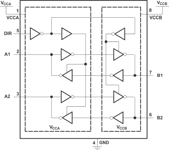
This 2-bit non-inverting bus transceiver uses two separate configurable power-supply rails. The A ports are designed to track VCCA and accepts any supply voltage from 1.2V to 3.6V. The B ports are designed to track VCCB and accepts any supply voltage from 1.2V to 3.6V. This allows for universal low-voltage bidirectional translation and level-shifting between any of the 1.2V, 1.5V, 1.8V, 2.5V, and 3.3V voltage nodes.
The SN74AVC2T45 is designed for asynchronous communication between two data buses. The logic levels of the direction-control (DIR pin) input activate either the B-port outputs or the A-port outputs. The device transmits data from the A bus to the B bus when the B-port outputs are activated and from the B bus to the A bus when the A-port outputs are activated. The input circuitry on both A and B ports always is active and must have a logic HIGH or LOW level applied to prevent excess leakage current on the internal CMOS structure.
| PART NUMBER | PACKAGE(1) | BODY SIZE (NOM) |
|---|---|---|
| SN74AVC2T45DCT | DCT, (SSOP, 8) | 2.95mm × 2.80mm |
| SN74AVC2T45DCU | DCU (VSSOP, 8) | 2.30mm × 2.00mm |
| SN74AVC2T45YZP | YZP (DSBGA, 8) | 1.89mm × 0.89mm |
| SN74AVC2T45DDF | DDF (SOT-23, 8) | 2.90mm × 1.60mm |
