SCES531M December 2003 – October 2024 SN74AVC2T45
PRODUCTION DATA
- 1
- 1 Features
- 2 Applications
- 3 Description
- 4 Pin Configuration and Functions
-
5 Specifications
- 5.1 Absolute Maximum Ratings
- 5.2 ESD Ratings
- 5.3 Recommended Operating Conditions
- 5.4 Thermal Information
- 5.5 Electrical Characteristics
- 5.6 Switching Characteristics: VCCA = 1.2 V
- 5.7 Switching Characteristics: VCCA = 1.5 V ±0.1 V
- 5.8 Switching Characteristics: VCCA = 1.8 V ±0.15 V
- 5.9 Switching Characteristics: VCCA = 2.5 V ±0.2 V
- 5.10 Switching Characteristics: VCCA = 3.3 V ±0.3 V
- 5.11 Operating Characteristics
- 5.12
Typical Characteristics
- 5.12.1 Typical Propagation Delay (A to B) vs Load Capacitance, TA = 25°C, VCCA = 1.2 V
- 5.12.2 Typical Propagation Delay (A to B) vs Load Capacitance, TA = 25°C, VCCA = 1.5 V
- 5.12.3 Typical Propagation Delay (A-to-B) vs Load Capacitance, TA = 25°C, VCCA = 1.8 V
- 5.12.4 Typical Propagation Delay (A to B) vs Load Capacitance, TA = 25°C, VCCA = 2.5 V
- 5.12.5 Typical Propagation Delay (A to B) vs Load Capacitance, TA = 25°C, VCCA = 3.3 V
- 6 Parameter Measurement Information
- 7 Detailed Description
- 8 Application and Implementation
- 9 Device and Documentation Support
- 10Revision History
- 11Mechanical, Packaging, and Orderable Information
Package Options
Refer to the PDF data sheet for device specific package drawings
Mechanical Data (Package|Pins)
- DCU|8
- DDF|8
- YZP|8
- DCT|8
Thermal pad, mechanical data (Package|Pins)
Orderable Information
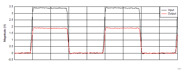
8.2.1.3 Application Curve
 Figure 8-2 3.3 V to 1.8 V Level-Shifting With 1-MHz Square Wave