SCES792C November 2009 – February 2024 SN74AVC4T245-Q1
PRODUCTION DATA
- 1
- 1 Features
- 2 Applications
- 3 Description
- 4 Pin Configuration and Functions
-
5 Specifications
- 5.1 Absolute Maximum Ratings
- 5.2 ESD Ratings
- 5.3 Recommended Operating Conditions
- 5.4 Thermal Information
- 5.5 Electrical Characteristics
- 5.6 Switching Characteristics: VCCA = 1.2V
- 5.7 Switching Characteristics, VCCA = 1.5V ± 0.1V
- 5.8 Switching Characteristics: VCCA = 1.8V ± 0.15V
- 5.9 Switching Characteristics: VCCA = 2.5V ± 0.2V
- 5.10 Switching Characteristics: VCCA = 3.3V ± 0.3V
- 5.11 Operating Characteristics
- 5.12 Typical Characteristics
- 6 Parameter Measurement Information
- 7 Detailed Description
- 8 Application and Implementation
- 9 Device and Documentation Support
- 10Revision History
- 11Mechanical, Packaging, and Orderable Information
Package Options
Refer to the PDF data sheet for device specific package drawings
Mechanical Data (Package|Pins)
- PW|16
- RGY|16
Thermal pad, mechanical data (Package|Pins)
- RGY|16
Orderable Information
3 Description
This 4-bit non-inverting bus
transceiver uses two separate configurable power-supply rails. The A port is
designed to track VCCA. VCCA accepts any supply voltage from
1.2V to 3.6V. The B port is designed to track VCCB. VCCB
accepts any supply voltage from
1.2V to 3.6V. The
SN74AVC4T245-Q1 is optimized to operate with
VCCA/VCCB set at 1.4V to 3.6V. It is operational with
VCCA/VCCB as low as 1.2V. This allows for universal
low-voltage bidirectional translation between any of the 1.2V, 1.5V, 1.8V, 2.5V,
and 3.3V voltage nodes.
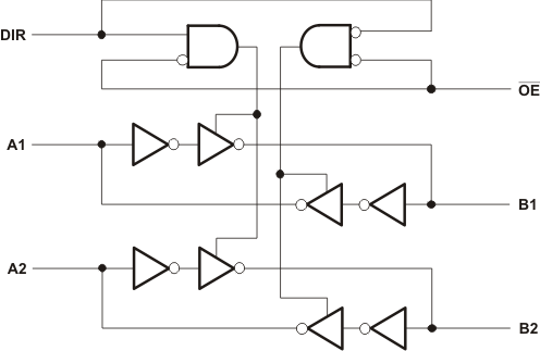
The SN74AVC4T245-Q1 is designed for asynchronous communication between two data buses. The logic levels of the direction-control (DIR) input and the output-enable ( OE) input activate either the B-port outputs or the A-port outputs or place both output ports into the high-impedance mode. The device transmits data from the A bus to the B bus when the B-port outputs are activated, and from the B bus to the A bus when the A-port outputs are activated. The input circuitry on both A and B ports is always active and must have a logic HIGH or LOW level applied to prevent excess ICC and ICCZ.
The SN74AVC4T245-Q1 is designed so that the control pins (1DIR, 2DIR, 1 OE, and 2 OE) are supplied by VCCA.
This device is fully specified for partial-power-down applications using Ioff. The Ioff circuitry disables the outputs, preventing damaging current backflow through the device when it is powered down.
The design of the VCC isolation feature places both ports in the high-impedance state if either VCC input is at GND.
To place the device in the high-impedance state during power up or power down, tie OE to VCC through a pullup resistor; the current-sinking capability of the driver determines the minimum value of the resistor.
| PART NUMBER | PACKAGE(1) | PACKAGE SIZE(2) |
|---|---|---|
| SN74AVC4T245-Q1 | RGY (VQFN, 16) | 4mm × 3.5mm |
| PW (TSSOP, 16) | 5mm × 6.4mm | |
| BQB (WQFN, 16) | 3.5mm × 2.5mm | |
| DYY (SOT, 16) | 4.2mm × 2mm |
 Logic Diagram (Positive Logic) for 1/2 of SN74AVC4T245-Q1