SCES901D February 2019 – January 2024 SN74AXC1T45-Q1
PRODUCTION DATA
- 1
- 1 Features
- 2 Applications
- 3 Description
- 4 Pin Configuration and Functions
- 5 Specifications
- 6 Parameter Measurement Information
-
7 Detailed Description
- 7.1 Overview
- 7.2 Functional Block Diagram
- 7.3
Feature Description
- 7.3.1 Standard CMOS Inputs
- 7.3.2 Balanced High-Drive CMOS Push-Pull Outputs
- 7.3.3 Partial Power Down (Ioff)
- 7.3.4 VCC Isolation
- 7.3.5 Over-voltage Tolerant Inputs
- 7.3.6 Negative Clamping Diodes
- 7.3.7 Fully Configurable Dual-Rail Design
- 7.3.8 I/Os with Integrated Static Pull-Down Resistors
- 7.3.9 Supports High-Speed Translation
- 7.4 Device Functional Modes
- 8 Application and Implementation
- 9 Device and Documentation Support
- 10Revision History
- 11Mechanical, Packaging, and Orderable Information
Package Options
Refer to the PDF data sheet for device specific package drawings
Mechanical Data (Package|Pins)
- DCK|6
- DRY|6
Thermal pad, mechanical data (Package|Pins)
- DRY|6
Orderable Information
8.2.1 Interrupt Request Application
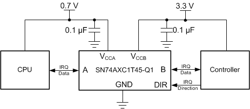
Figure 8-1 shows an example of the SN74AXC1T45-Q1 being used in an application where a system controller flags an interrupt request (IRQ) to the CPU. The system controller determines the direction of the IRQ line to either flag an interrupt to the CPU or allow the CPU to drive data on the line. In this application the controller is operating at 3.3V while the CPU can operate as low as 0.65V.
The SN74AXC1T45-Q1 device is used to allow these devices to communicate at the appropriate voltage levels. Because the SN74AXC1T45-Q1 does not have an output-enable (OE) pin, the system designer should take precautions to avoid bus contention between the CPU and controller when changing directions.
 Figure 8-1 Interrupt Request Application