SCES892D November 2018 – January 2024 SN74AXC8T245-Q1
PRODUCTION DATA
- 1
- 1 Features
- 2 Applications
- 3 Description
- 4 Pin Configuration and Functions
-
5 Specifications
- 5.1 Absolute Maximum Ratings
- 5.2 ESD Ratings
- 5.3 Recommended Operating Conditions
- 5.4 Thermal Information
- 5.5 Electrical Characteristics
- 5.6 Switching Characteristics, VCCA = 0.7V
- 5.7 Switching Characteristics, VCCA = 0.8V
- 5.8 Switching Characteristics, VCCA = 0.9V
- 5.9 Switching Characteristics, VCCA = 1.2V
- 5.10 Switching Characteristics, VCCA = 1.5V
- 5.11 Switching Characteristics, VCCA = 1.8V
- 5.12 Switching Characteristics, VCCA = 2.5V
- 5.13 Switching Characteristics, VCCA = 3.3V
- 5.14 Operating Characteristics: TA = 25°C
- 5.15 Typical Characteristics
- 6 Parameter Measurement Information
- 7 Detailed Description
- 8 Application and Implementation
- 9 Device and Documentation Support
- 10Revision History
- 11Mechanical, Packaging, and Orderable Information
Package Options
Mechanical Data (Package|Pins)
Thermal pad, mechanical data (Package|Pins)
- RGY|24
Orderable Information
4 Pin Configuration and Functions
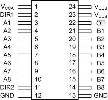
 Figure 4-1 PW Package, 24-Pin TSSOP
(Top View)
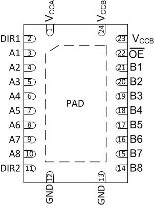
PAD — may be grounded
(recommended) or left floating.
Figure 4-2 RHL and WRGY Package, 24-Pin VQFN (Top
View)Table 4-1 Pin Functions
| PIN | TYPE(1) | DESCRIPTION | |
|---|---|---|---|
| NAME | NO. | ||
| A1 | 3 | I/O | Input/output A1. Referenced to VCCA. |
| A2 | 4 | I/O | Input/output A2. Referenced to VCCA. |
| A3 | 5 | I/O | Input/output A3. Referenced to VCCA. |
| A4 | 6 | I/O | Input/output A4. Referenced to VCCA. |
| A5 | 7 | I/O | Input/output A5. Referenced to VCCA. |
| A6 | 8 | I/O | Input/output A6. Referenced to VCCA. |
| A7 | 9 | I/O | Input/output A7. Referenced to VCCA. |
| A8 | 10 | I/O | Input/output A8. Referenced to VCCA. |
| B1 | 21 | I/O | Input/output B1. Referenced to VCCB. |
| B2 | 20 | I/O | Input/output B2. Referenced to VCCB. |
| B3 | 19 | I/O | Input/output B3. Referenced to VCCB. |
| B4 | 18 | I/O | Input/output B4. Referenced to VCCB. |
| B5 | 17 | I/O | Input/output B5. Referenced to VCCB. |
| B6 | 16 | I/O | Input/output B6. Referenced to VCCB. |
| B7 | 15 | I/O | Input/output B7. Referenced to VCCB. |
| B8 | 14 | I/O | Input/output B8. Referenced to VCCB. |
| DIR1 | 2 | I | Direction-control signal 1. Referenced to VCCA. Refer to Table 7-1. |
| DIR2 | 11 | I | Direction-control signal 2. Refer to Table 7-1. Referenced to VCCA. Tie to GND to maintain backward compatibility with SN74AVC8T245-Q1 device. |
| GND | 12 | — | Ground |
| 13 | — | Ground | |
| OE | 22 | I | Output Enable. Pull to GND to enable all outputs. Pull to VCCA to place all outputs in high-impedance mode. Referenced to VCCA. Refer to Table 7-1. |
| VCCA | 1 | — | A-port supply voltage. 0.65V ≤ VCCA ≤ 3.6V |
| VCCB | 23 | — | B-port supply voltage. 0.65V ≤ VCCB ≤ 3.6V |
| 24 | — | B-port supply voltage. 0.65V ≤ VCCB ≤ 3.6V | |
(1) PAD - may be grounded (recommended) or left floating.