SCDS167A May 2004 – July 2022 SN74CB3Q16211
PRODUCTION DATA
- 1 Features
- 2 Applications
- 3 Description
- 4 Revision History
- 5 Description (continued)
- 6 Pin Configuration and Functions
- 7 Specifications
- 8 Parameter Measurement Information
- 9 Device and Documentation Support
- 10Mechanical, Packaging, and Orderable Information
Package Options
Mechanical Data (Package|Pins)
Thermal pad, mechanical data (Package|Pins)
Orderable Information
6 Pin Configuration and Functions
 Figure 6-1 DGG, DGV, or DL Package, 56-Pin TSSOP
and TVSOP (Top View)
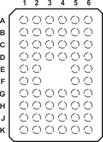
 Figure 6-2 ZQL Package, 56-Pin BGA (Top
View)
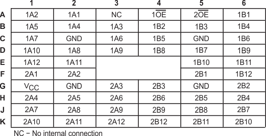
 Figure 6-3 Functions Table