SCDS141D October 2003 – September 2021 SN74CB3Q3305
PRODUCTION DATA
- 1 Features
- 2 Applications
- 3 Description
- 4 Revision History
- 5 Pin Configuration and Functions
- 6 Specifications
- 7 Parameter Measurement Information
- 8 Detailed Description
- 9 Application and Implementation
- 10Power Supply Recommendations
- 11Layout
- 12Device and Documentation Support
- 13Mechanical, Packaging, and Orderable Information
Package Options
Refer to the PDF data sheet for device specific package drawings
Mechanical Data (Package|Pins)
- DCU|8
- PW|8
Thermal pad, mechanical data (Package|Pins)
Orderable Information
3 Description
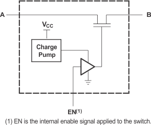
The SN74CB3Q3305 device is a high-bandwidth FET bus switch using a charge pump to elevate the gate voltage of the pass transistor, providing a low and flat ON-state resistance (ron). The low and flat ON-state resistance allows for minimal propagation delay and supports switching input voltage beyond the supply on the data input/output (I/O) ports. The device also features low data I/O capacitance to minimize capacitive loading and signal distortion on the data bus. Specifically designed to support high-bandwidth applications, the SN74CB3Q3305 device provides an optimized interface solution ideally suited for broadband communications, networking, and data-intensive computing systems.
This device is fully specified for partial-power-down applications using Ioff. The Ioff circuitry prevents damaging current backflow through the device when it is powered down. The device has isolation during power off.
To ensure the high-impedance state during power up or power down, OE should be tied to GND through a pulldown resistor; the minimum value of the resistor is determined by the current-sourcing capability of the driver.
| PART NUMBER | PACKAGE | BODY SIZE (NOM) |
|---|---|---|
| SN74CB3Q3305 | VSSOP (8) | 2.00 mm × 3.10 mm |
| TSSOP (8) | 3.00 mm × 6.10 mm |
 Simplified Schematic, Each FET Switch (SW)