SCDS119C january 2003 – December 2015 SN74CB3T3306
PRODUCTION DATA.
- 1 Features
- 2 Applications
- 3 Description
- 4 Revision History
- 5 Pin Configuration and Functions
- 6 Specifications
- 7 Parameter Measurement Information
- 8 Detailed Description
- 9 Application and Implementation
- 10Power Supply Recommendations
- 11Layout
- 12Device and Documentation Support
- 13Mechanical, Packaging, and Orderable Information
Package Options
Mechanical Data (Package|Pins)
Thermal pad, mechanical data (Package|Pins)
Orderable Information
9 Application and Implementation
NOTE
Information in the following applications sections is not part of the TI component specification, and TI does not warrant its accuracy or completeness. TI’s customers are responsible for determining suitability of components for their purposes. Customers should validate and test their design implementation to confirm system functionality.
9.1 Application Information
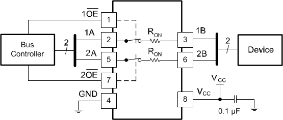
This application is specifically to connect a 5-V bus to a 3.3 V device. Ideally, set VCC to 3.3 V. It is assumed that communication in this particular application is one-directional, going from the bus controller to the device.
9.2 Typical Application
 Figure 8. Typical Application Diagram
9.2.1 Design Requirements
This device uses CMOS technology and has balanced output drive. Take care to avoid bus contention because it can drive currents that would exceed maximum limits.
Because this design is for down-translating voltage, no pull-up resistors are required.
9.2.2 Detailed Design Procedure
- Recommended Input conditions
- Specified high and low levels. See (VIH and VIL) in Recommended Operating Conditions
- Inputs are overvoltage tolerant allowing them to go as high as 7 V at any valid VCC
- Recommend output conditions
- Load currents should not exceed 128 mA on each channel
9.2.3 Application Curves
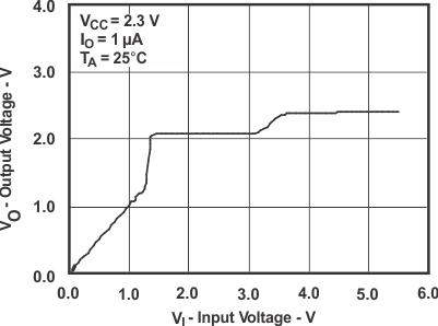
 Figure 9. Data Output Voltage vs Data Input Voltage
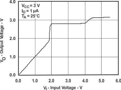
 Figure 10. Data Output Voltage vs Data Input Voltage