SCDS001O November 1992 – September 2015 SN74CBT3244
PRODUCTION DATA.
- 1 Features
- 2 Applications
- 3 Description
- 4 Revision History
- 5 Pin Configuration and Functions
- 6 Specifications
- 7 Parameter Measurement Information
- 8 Detailed Description
- 9 Application and Implementation
- 10Power Supply Recommendations
- 11Layout
- 12Device and Documentation Support
- 13Mechanical, Packaging, and Orderable Information
Package Options
Refer to the PDF data sheet for device specific package drawings
Mechanical Data (Package|Pins)
- DGV|20
- DB|20
- DW|20
- PW|20
- RGY|20
Thermal pad, mechanical data (Package|Pins)
Orderable Information
8 Detailed Description
8.1 Overview
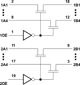
The SN74CBT3244 has eight bits of high-speed TTL-compatible bus switching. The switches are grouped in the 2 groups of 4 bits each. Each group has output-enabled inputs to allow signals to pass between A and B ports. The signals can travel from A port to B port or vice versa.
The low ON-state resistance of the switch allows connections to be made with minimal propagation delay. The device is ideal for switching high speed digital signals between microprocessors and peripheral devices which is useful in test applications, measurement applications, and control boards for factory automation.
8.2 Functional Block Diagram
 Figure 3. Simplified Schematic
8.3 Feature Description
The SN74CBT3244 device support same pin configuration as industry standard '244. This device has a near zero propagation delay allowing high speed signal switching up to 200 Mhz. The signals see lower distortion since the device has low ON-resistance (5 Ω) coupled with low-output capacitance (6 pF) . SN74CBT3244 has a very low power consumption in idle state consuming ICC of 50 µA only allowing power-saving for the system. The device supports signal inputs any where between 0 V to 5 V.
8.4 Device Functional Modes
The device is organized as two 4-bit low-impedance switches with separate output-enable (OE) inputs.The Output Enable OE is active low, implying when low A port is connected to B port. This switch is bidirectional in nature. Asserting OE high will disconnect A port from B port. To ensure the high-impedance state during power up or power down, OE should be tied to VCC through a pullup resistor. The minimum value of the resistor is determined by the current-sinking capability of the driver.
Table 1. Function Table
(Each 4-Bit Bus Switch)
| INPUT OE | FUNCTION | |||
|---|---|---|---|---|
| L | A port = B port | |||
| H | Disconnect | |||