SCDS047H March 1998 – December 2018 SN74CBTLV3383
PRODUCTION DATA.
- 1 Features
- 2 Applications
- 3 Description
- 4 Revision History
- 5 Pin Configuration and Functions
- 6 Specifications
- 7 Parameter Measurement Information
- 8 Detailed Description
- 9 Application and Implementation
- 10Power Supply Recommendations
- 11Layout
- 12Device and Documentation Support
- 13Mechanical, Packaging, and Orderable Information
Package Options
Refer to the PDF data sheet for device specific package drawings
Mechanical Data (Package|Pins)
- DGV|24
- DBQ|24
- DW|24
- PW|24
Thermal pad, mechanical data (Package|Pins)
Orderable Information
7 Parameter Measurement Information
 Figure 1. Load Current
 Figure 2. Voltage Waveforms Pulse Duration Figure 2. Voltage Waveforms Pulse Duration
xx |
 Figure 3. Voltage Waveforms Setup and Hold Times Figure 3. Voltage Waveforms Setup and Hold Times |
 Figure 4. Voltage Waveforms Propagation Delay Times Inverting and Noninverting Outputs Figure 4. Voltage Waveforms Propagation Delay Times Inverting and Noninverting Outputs |
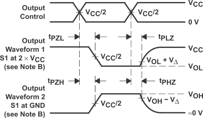
 Figure 5. Voltage Waveforms Enable And Disable Times Low- and High-Level Enabling Figure 5. Voltage Waveforms Enable And Disable Times Low- and High-Level Enabling |
Notes:
- CL includes probe and jig capacitance.
- Waveform 1 is for an output with internal conditions such that the output is low except when disabled by the output control. Waveform 2 is for an output with internal conditions such that the output is high except when disabled by the output control
- All input pulses are supplied by generators having the following characteristics: PRR ≤ 10 MHz, ZO = 50 Ω, tr ≤ 2 ns, tf ≤ 2 ns.
- The outputs are measured one at a time with one transition per measurement.
- tPLZ and tPHZ are the same as tdis.
- tPZL and tPZH are the same as ten.
- tPLH and tPHL are the same as tpd.
- H. All parameters and waveforms are not applicable to all devices.