SCDS192C April   2005  – September 2021 SN74CBTU4411

PRODUCTION DATA  

  1. Features
  2. Applications
  3. Description
  4. Revision History
  5. Pin Configuration and Functions
  6. Specifications
    1. 6.1 Absolute Maximum Ratings
    2. 6.2 ESD Ratings
    3. 6.3 Recommended Operating Conditions
    4. 6.4 Thermal Information
    5. 6.5 Electrical Characteristics
    6. 6.6 Switching Characteristics
    7. 6.7 Typical Characteristic
  7. Parameter Measurement Information
    1. 7.1 Enable and Disable Times
    2. 7.2 Skew and Propagation Delay Times
  8. Detailed Description
    1. 8.1 Overview
    2. 8.2 Functional Block Diagram
    3. 8.3 Feature Description
    4. 8.4 Device Functional Modes
  9. Application and Implementation
    1. 9.1 Application Information
    2. 9.2 Typical Application
      1. 9.2.1 Design Requirements
      2. 9.2.2 Detailed Design Procedure
      3. 9.2.3 Application Curve
  10. 10Power Supply Recommendations
  11. 11Layout
    1. 11.1 Layout Guidelines
    2. 11.2 Layout Example
  12. 12Device and Documentation Support
    1. 12.1 Documentation Support
      1. 12.1.1 Related Documentation
    2. 12.2 Receiving Notification of Documentation Updates
    3. 12.3 Support Resources
    4. 12.4 Trademarks
  13. 13Electrostatic Discharge Caution
  14. 14Glossary
  15. 15Mechanical, Packaging, and Orderable Information

Package Options

Mechanical Data (Package|Pins)
Thermal pad, mechanical data (Package|Pins)
Orderable Information

Description

The SN74CBTU4411 device is a high-bandwidth, SSTL_18 compatible FET multiplexer/demultiplexer with low ON-state resistance (ron). The device uses an internal charge pump to elevate the gate voltage of the pass transistor, providing a low and flat ron. The low and flat ron allows for minimal propagation delay and supports rail-to-rail signaling on data input/output (I/O) ports. The device also features very low data I/O capacitance to minimize capacitive loading and signal distortion on the data bus. Matched ron and I/O capacitance among channels results in extremely low differential and rising or falling edge skew. This allows the device to show optimal performance in DDR-II applications.

Device Information(1)
PART NUMBER PACKAGE BODY SIZE
SN74CBTU4411ZST NFBGA (72) 7.00 mm × 7.00 mm
For all available packages, see the orderable addendum at the end of the data sheet.
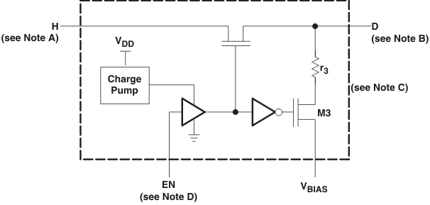
GUID-C9E6E521-8A4F-4BAF-9B91-57CF960E8E33-low.gif
Applicable for ports H0 through H9
Applicable for ports D0 through D9
r3 + ron (M3) = 400 Ω typical.
EN is the internal enable signal applied to the switch.
Simplified Schematic, Each FET Switch (SW1)
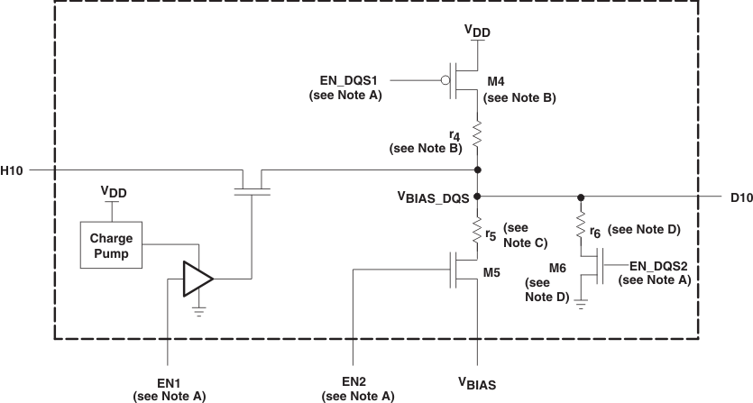
GUID-5ACBFA35-354F-4FB7-9A70-5602001E8815-low.gif
EN_DQS1, EN_DQS2, EN1, and EN2 are the internal enable signals applied to the switch.
r4 + ron (M4) = 1 kΩ typical.
r5 + ron (M5) = 400 Ω typical.
r6 + ron (M6) = 2.3 kΩ typical.
Simplified Schematic, Each FET Switch (SW2)