SCDS192C April 2005 – September 2021 SN74CBTU4411
PRODUCTION DATA
- 1 Features
- 2 Applications
- 3 Description
- 4 Revision History
- 5 Pin Configuration and Functions
- 6 Specifications
- 7 Parameter Measurement Information
- 8 Detailed Description
- 9 Application and Implementation
- 10Power Supply Recommendations
- 11Layout
- 12Device and Documentation Support
- 13Electrostatic Discharge Caution
- 14Glossary
- 15Mechanical, Packaging, and Orderable Information
Package Options
Mechanical Data (Package|Pins)
- ZST|72
Thermal pad, mechanical data (Package|Pins)
Orderable Information
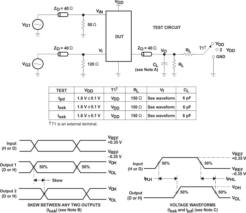
7.2 Skew and Propagation Delay Times

CL includes probe and jig capacitance.
tosk is the difference in output voltage from channel to channel in a specific device.
tPLH and tPHL are the same as tpd and tesk = |tPLH – tPHL|
All input pulses are supplied by generators having the following characteristics: ZOS = 50 Ω, rising and falling edge rate is 1 V/ns.
The outputs are measured one at a time, with one transition per measurement.
Figure 7-2 Test Circuit and Voltage Waveforms