SCLS113E December 1982 – February 2022 SN54HC157 , SN74HC157
PRODUCTION DATA
- 1 Features
- 2 Description
- 3 Revision History
- 4 Pin Configuration and Functions
- 5 Specifications
- 6 Parameter Measurement Information
- 7 Detailed Description
- 8 Power Supply Recommendations
- 9 Layout
- 10Device and Documentation Support
- 11Mechanical, Packaging, and Orderable Information
Package Options
Refer to the PDF data sheet for device specific package drawings
Mechanical Data (Package|Pins)
- DB|16
- PW|16
- NS|16
- N|16
- D|16
Thermal pad, mechanical data (Package|Pins)
Orderable Information
6 Parameter Measurement Information
tpd is the maximum between tPLH and tPHL
 Figure 6-1 Load Circuit
 Figure 6-3 Voltage Waveform
Input Rise and Fall Times
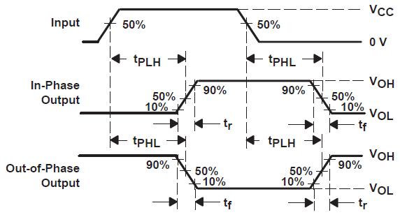
 Figure 6-2 Voltage Waveforms
Propagation Delay and Output Transition Times
A. CL includes probe and test-fixture capacitance.
B. Phase relationships between waveforms were chosen arbitrarily. All input pulses are supplied by generators having the following charactersitics: PRR ≤ 1 MHz, ZO = 50 Ω, tr = 6 ns, tf = 6 ns.
C. The outputs are measured one at a time with one input transition per measurement.