SCLS946 august 2023 SN74HC165B-EP
PRODUCTION DATA
- 1
- 1 Features
- 2 Applications
- 3 Description
- 4 Revision History
- 5 Pin Configuration and Functions
-
6 Specifications
- 6.1 Absolute Maximum Ratings
- 6.2 ESD Ratings
- 6.3 Recommended Operating Conditions
- 6.4 Thermal Information
- 6.5 Electrical Characteristics
- 6.6 Timing Requirements, VCC = 2 V
- 6.7 Timing Requirements, VCC = 4.5 V
- 6.8 Timing Requirements, VCC = 6 V
- 6.9 Switching Characteristics, VCC = 2 V
- 6.10 Switching Characteristics, VCC = 4.5 V
- 6.11 Switching Characteristics, VCC = 6 V
- 6.12 Operating Characteristics
- 6.13 Typical Characteristics
- 7 Parameter Measurement Information
- 8 Detailed Description
- 9 Application and Implementation
- 10Device and Documentation Support
- 11Mechanical, Packaging, and Orderable Information
Package Options
Mechanical Data (Package|Pins)
- PW|16
Thermal pad, mechanical data (Package|Pins)
Orderable Information
6.8 Timing Requirements, VCC = 6 V
over recommended operating free-air temperature range (unless otherwise noted) (see Section 7)
| PARAMETER | TEST CONDITION | 25°C | –55°C to 125°C | UNIT | |||
|---|---|---|---|---|---|---|---|
| MIN | MAX | MIN | MAX | ||||
| fclock | Clock frequency | 36 | 25 | MHz | |||
| tw | Pulse duration | CLK high or low | 14 | 20 | ns | ||
| SH/ LD low | 14 | 20 | |||||
| tsu | Setup time | SH/ LD high before CLK↑ | 14 | 20 | ns | ||
| SER before CLK↑ | 7 | 10 | |||||
| CLK INH before CLK↑ | 17 | 25 | |||||
| Data before SH/ LD↑ | 17 | 26 | |||||
| th | Hold time | SER data after CLK↑ | 5 | 5 | ns | ||
| Parallel data after SH/ LD↑ | 5 | 5 | |||||
| SH/ LD high after CLK↑ | 5 | 5 | |||||
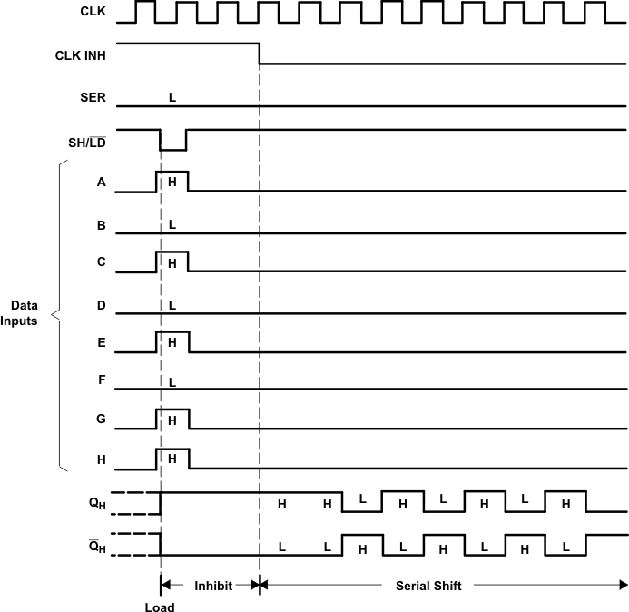
 Figure 6-1 Typical Shift, Load, and Inhibit Sequences