SCLS543C September 2002 – June 2022 SN74HC244-Q1
PRODUCTION DATA
- 1 Features
- 2 Description
- 3 Revision History
- 4 Pin Configuration and Functions
- 5 Specifications
- 6 Parameter Measurement Information
- 7 Detailed Description
- 8 Power Supply Recommendations
- 9 Layout
- 10Device and Documentation Support
- 11Mechanical, Packaging, and Orderable Information
Package Options
Refer to the PDF data sheet for device specific package drawings
Mechanical Data (Package|Pins)
- DW|20
- PW|20
Thermal pad, mechanical data (Package|Pins)
Orderable Information
2 Description
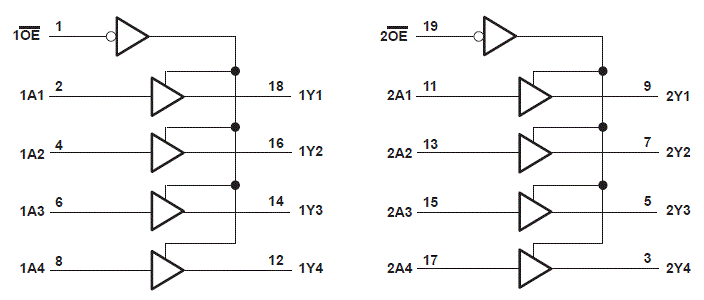
This octal buffer and line driver is designed specifically to improve both the performance and density of 3-state memory address drivers, clock drivers, and bus-oriented receivers and transmitters. The SN74HC244 is organized as two 4-bit buffers/drivers with separate output-enable (OE) inputs. When OE is low, the device passes noninverted data from the A inputs to the Y outputs. When OE is high, the outputs are in the high-impedance state.
Device Information
| PART NUMBER | PACKAGE(1) | BODY SIZE (NOM) |
|---|---|---|
| SN74HC244QDW-Q1 | SOIC (20) | 12.80 mm × 7.50 mm |
| SN74HC244QPW-Q1 | TSSOP (20) | 6.50 mm × 4.40 mm |
(1) For all available packages, see
the orderable addendum at the end of the data sheet.
 Functional Block Diagram