SCLS134F December 1982 – March 2022 SN54HC259 , SN74HC259
PRODUCTION DATA
- 1 Features
- 2 Description
- 3 Revision History
- 4 Pin Configuration and Functions
- 5 Specifications
- 6 Parameter Measurement Information
- 7 Detailed Description
- 8 Power Supply Recommendations
- 9 Layout
- 10Device and Documentation Support
- 11Mechanical, Packaging, and Orderable Information
Package Options
Refer to the PDF data sheet for device specific package drawings
Mechanical Data (Package|Pins)
- PW|16
- DYY|16
- NS|16
- N|16
- D|16
Thermal pad, mechanical data (Package|Pins)
Orderable Information
2 Description
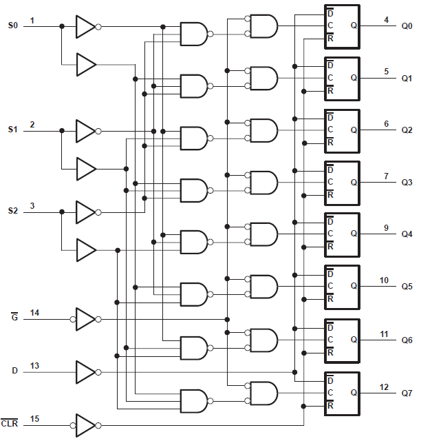
These 8-bit addressable latches are designed for general-purpose storage applications in digital systems. Specific uses include working registers, serial-holding registers, and active-high decoders or demultiplexers. They are multifunctional devices capable of storing single-line data in eight addressable latches and being a 1-of-8 decoder or demultiplexer with active-high outputs.
| PART NUMBER | PACKAGE(1) | BODY SIZE (NOM) |
|---|---|---|
| SN74HC259D | SOIC (16) | 9.90 mm × 3.90 mm |
| SN74HC259N | PDIP (16) | 19.31 mm × 6.35 mm |
| SN74HC259NS | SO (16) | 6.20 mm × 5.30 mm |
| SN74HC259PW | TSSOP (16) | 5.00 mm × 4.40 mm |
| SN54HC259J | CDIP (16) | 24.38 mm × 6.92 mm |
| SNJ54HC259FK | LCCC (20) | 8.89 mm × 8.45 mm |

Pin numbers are for the D, J, N, NS, PW, and W packages.
Functional Block Diagram