SCLS143E December 1982 – December 2024 SN54HC393 , SN74HC393
PRODUCTION DATA
- 1
- 1 Features
- 2 Description
- 3 Pin Configuration and Functions
- 4 Specifications
- 5 Parameter Measurement Information
- 6 Detailed Description
- 7 Application and Implementation
- 8 Device and Documentation Support
- 9 Revision History
- 10Mechanical, Packaging, and Orderable Information
Package Options
Refer to the PDF data sheet for device specific package drawings
Mechanical Data (Package|Pins)
- D|14
- DYY|14
- DB|14
- PW|14
- N|14
- NS|14
Thermal pad, mechanical data (Package|Pins)
Orderable Information
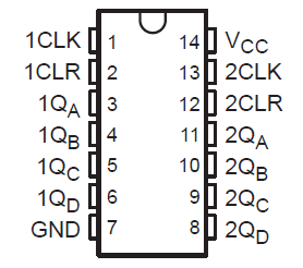
3 Pin Configuration and Functions
 SN54HC393 J or W Package, 14-Pin CDIP or CFP;
SN74HC393 D, DB, DYY, N, NS, or PW Package; 14-Pin SOIC, SSOP, SOT-23, TVSOP, SOP, or TSSOP
(Top View)

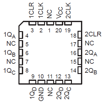
A. NC - No
internal connection
SN54HC393 FK Package, 20-Pin LCCC(Top View)
Table 3-1 Pin Functions
| PIN | TYPE1 | DESCRIPTION | |
|---|---|---|---|
| NAME | NO. | ||
| 1CLK | 1 | I | Counter 1 Clock Input |
| 1CLR | 2 | I | Counter 1 Clear Input |
| 1QA | 3 | O | Counter 1 A Output |
| 1QB | 4 | O | Counter 1 B Output |
| 1QC | 5 | O | Counter 1 B Output |
| 1QD | 6 | O | Counter 1 B Output |
| GND | 7 | G | Ground |
| 2QD | 8 | O | Counter 2 D Output |
| 2QC | 9 | O | Counter 2 C Output |
| 2QB | 10 | O | Counter 2 B Output |
| 2QA | 11 | O | Counter 2 A Output |
| 2CLR | 12 | I | Counter 2 Clear Input |
| 2CLK | 13 | I | Counter 2 Clock Input |
| VCC | 14 | P | VCC |
- I = Input, O = Output, I/O = Input or Output, G = Ground, P = Power.