SCLS542C September 2003 – June 2024 SN74HC4851
PRODUCTION DATA
- 1
- 1 Features
- 2 Applications
- 3 Description
- 4 Pin Configuration and Functions
- 5 Specifications
- 6 Parameter Measurement Information
- 7 Detailed Description
- 8 Application and Implementation
- 9 Device and Documentation Support
- 10Revision History
- 11Mechanical, Packaging, and Orderable Information
Package Options
Refer to the PDF data sheet for device specific package drawings
Mechanical Data (Package|Pins)
- PW|16
- N|16
- D|16
- DGV|16
Thermal pad, mechanical data (Package|Pins)
Orderable Information
8.1 Application Information
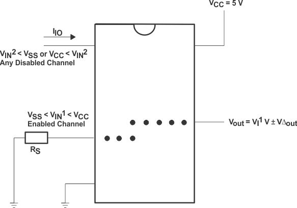
 Figure 8-1 Injection-Current Coupling Specification
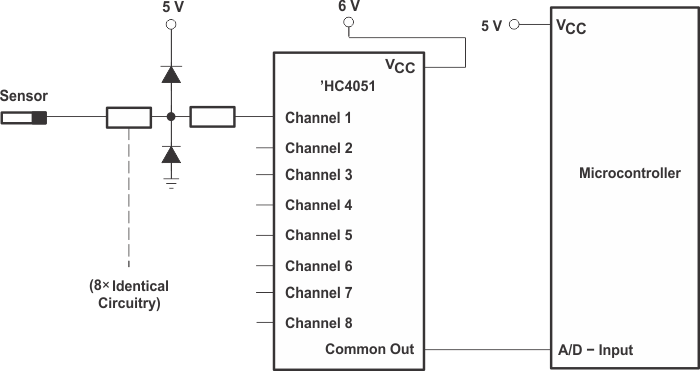
 Figure 8-2 Alternate
Solution Requires 32 Passive Components and One Extra 6-V Regulator to Suppress
Injection Current Into a Standard ’HC4051 Multiplexer
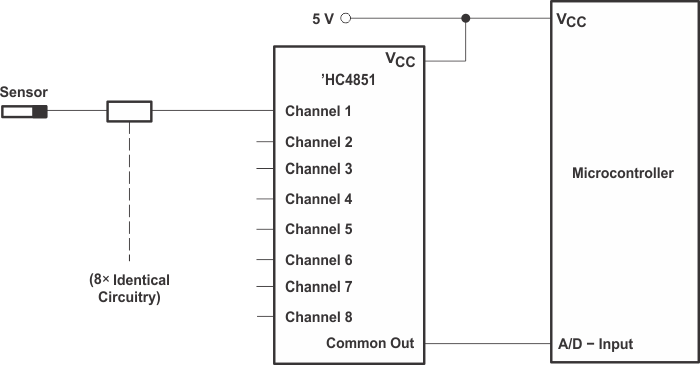
 Figure 8-3 Solution
by Applying the ’HC4851 Multiplexer
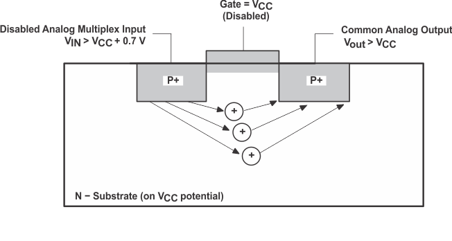
 Figure 8-4 Diagram
of Bipolar Coupling Mechanism (Appears if VIN Exceeds VCC,
Driving Injection Current Into the Substrate)