SCLS542C September 2003 – June 2024 SN74HC4851
PRODUCTION DATA
- 1
- 1 Features
- 2 Applications
- 3 Description
- 4 Pin Configuration and Functions
- 5 Specifications
- 6 Parameter Measurement Information
- 7 Detailed Description
- 8 Application and Implementation
- 9 Device and Documentation Support
- 10Revision History
- 11Mechanical, Packaging, and Orderable Information
Package Options
Refer to the PDF data sheet for device specific package drawings
Mechanical Data (Package|Pins)
- PW|16
- N|16
- D|16
- DGV|16
Thermal pad, mechanical data (Package|Pins)
Orderable Information
4 Pin Configuration and Functions
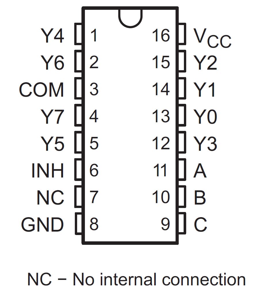
 Figure 4-1 SN74HC4851 PW
Package, 16-Pin TSSOP (Top View)
Figure 4-1 SN74HC4851 PW
Package, 16-Pin TSSOP (Top View)Table 4-1 Function Table
| Inputs | On Channel | |||
|---|---|---|---|---|
| INH | C | B | A | Yx |
| L | L | L | L | Y0 |
| L | L | L | H | Y1 |
| L | L | H | L | Y2 |
| L | L | H | H | Y3 |
| L | H | L | L | Y4 |
| L | H | L | H | Y5 |
| L | H | H | L | Y6 |
| L | H | H | H | Y7 |
| H | X | X | X | None |