SCLS573A March 2004 – June 2024 SN74HC4852
PRODUCTION DATA
- 1
- 1 Features
- 2 Applications
- 3 Description
- 4 Pin Configuration and Functions
- 5 Specifications
- 6 Parameter Measurement Information
- 7 Detailed Description
- 8 Application and Implementation
- 9 Device and Documentation Support
- 10Revision History
- 11Mechanical, Packaging, and Orderable Information
Package Options
Refer to the PDF data sheet for device specific package drawings
Mechanical Data (Package|Pins)
- PW|16
- N|16
- D|16
- DGV|16
Thermal pad, mechanical data (Package|Pins)
- D|16
Orderable Information
6 Parameter Measurement Information
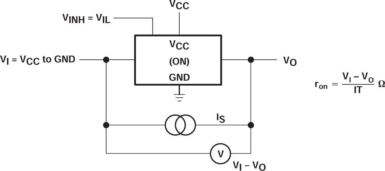 Figure 6-1 On-State Resistance Test Circuit
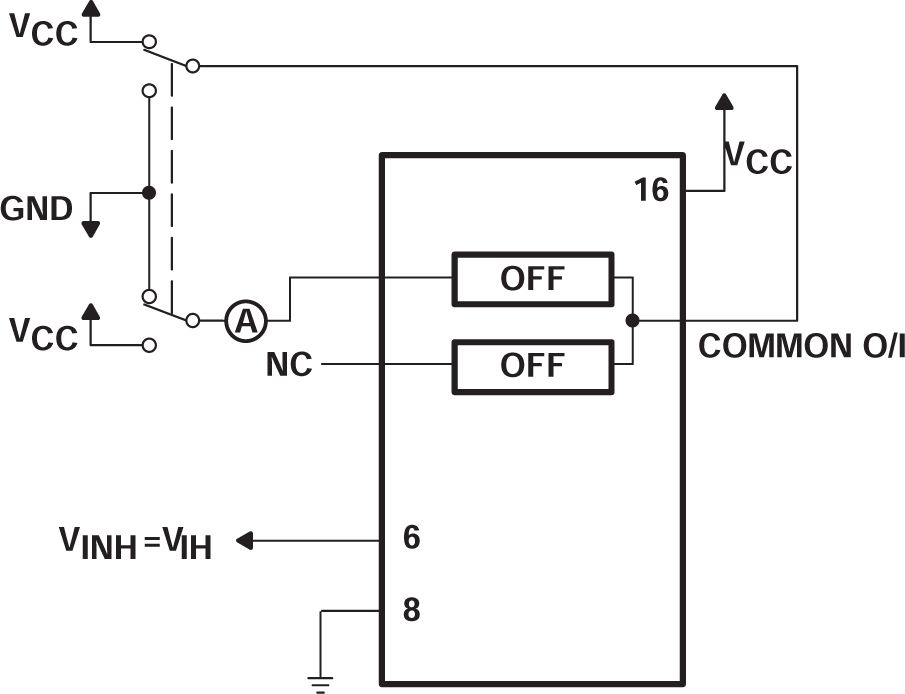 Figure 6-2 Maximum Off-Channel Leakage Current, Any One Channel, Test Setup
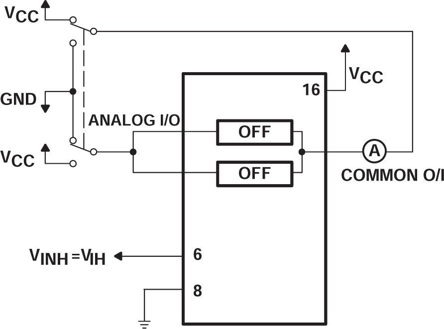 Figure 6-3 Maximum Off-Channel Leakage Current, Common Channel, Test Setup
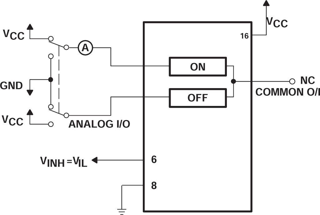 Figure 6-4 Maximum On-Channel Leakage Current, Channel to Channel, Test Setup
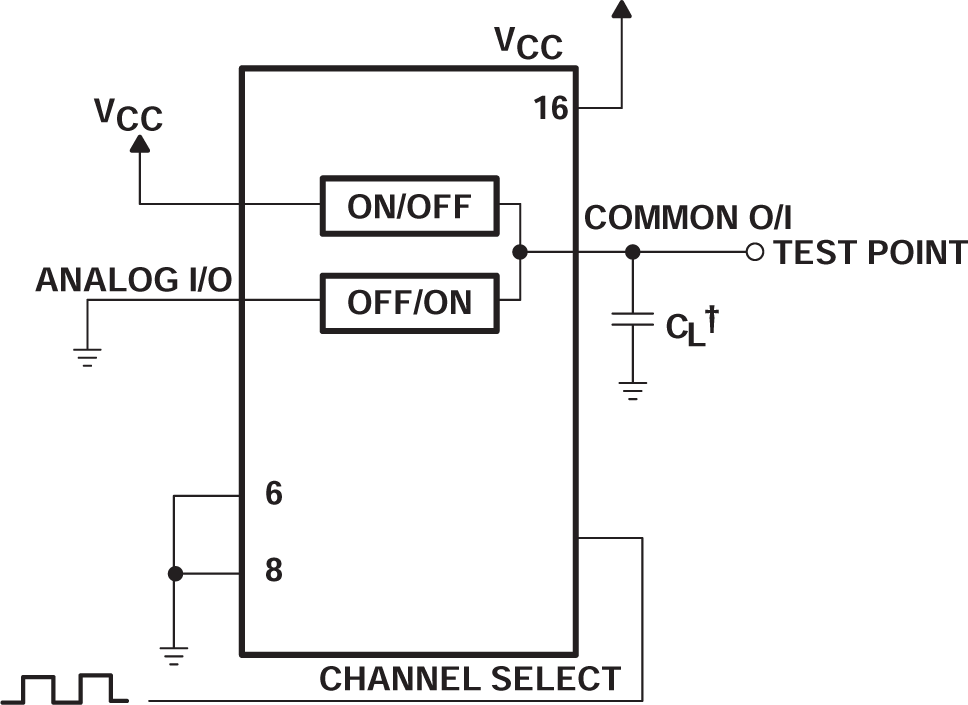
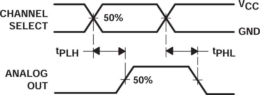 Figure 6-5 Propagation Delays, Channel Select to Analog Out
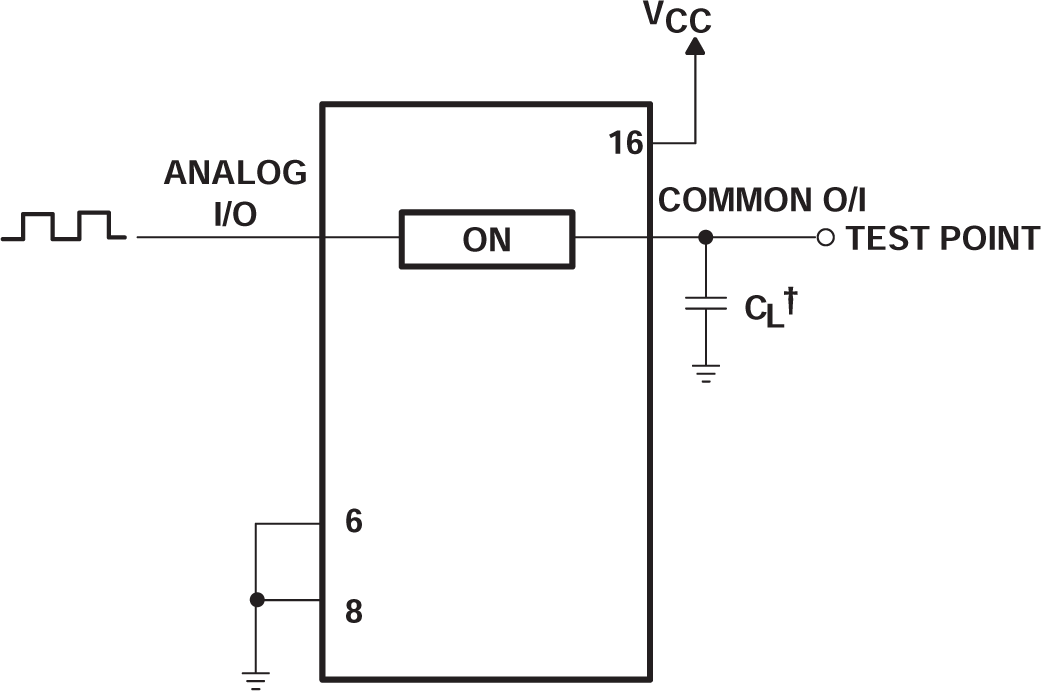
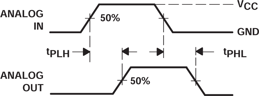 Figure 6-7 Propagation Delays, Analog in to Analog Out
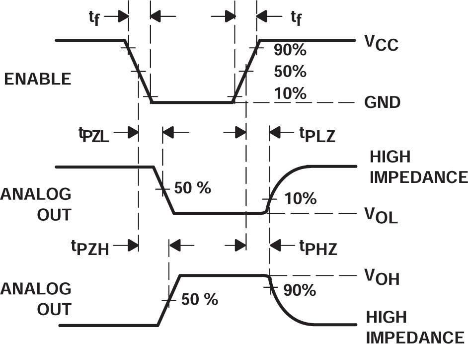 Figure 6-9 Propagation Delays, Enable to Analog Out
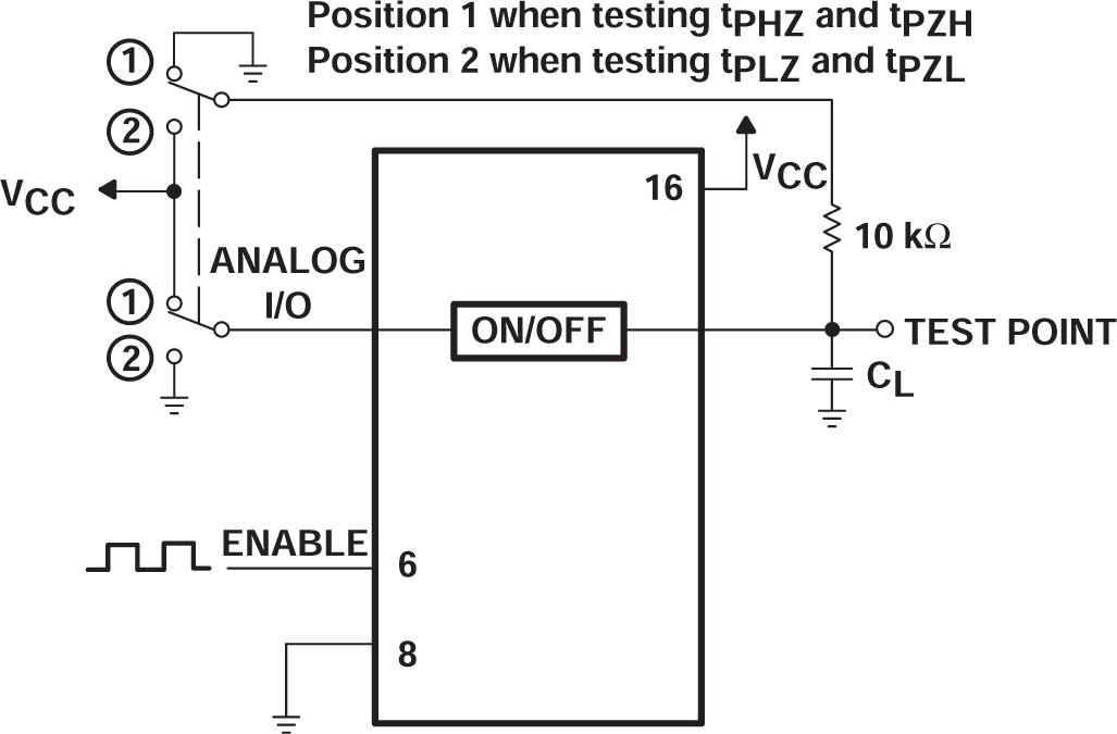 Figure 6-10 Propagation Delay, Enable to Analog Out, Test Setup
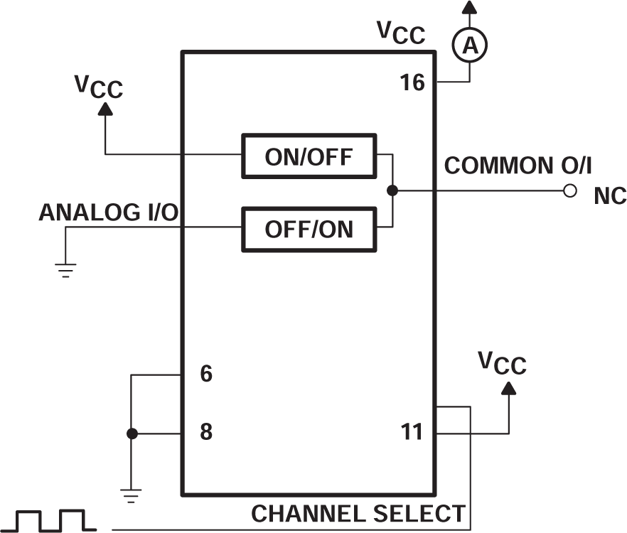 Figure 6-11 Power-Dissipation Capacitance, Test Setup
†. Includes all probe and jig capacitance
†. Includes all probe and jig capacitance
