SCLS573A March 2004 – June 2024 SN74HC4852
PRODUCTION DATA
- 1
- 1 Features
- 2 Applications
- 3 Description
- 4 Pin Configuration and Functions
- 5 Specifications
- 6 Parameter Measurement Information
- 7 Detailed Description
- 8 Application and Implementation
- 9 Device and Documentation Support
- 10Revision History
- 11Mechanical, Packaging, and Orderable Information
Package Options
Refer to the PDF data sheet for device specific package drawings
Mechanical Data (Package|Pins)
- PW|16
- N|16
- D|16
- DGV|16
Thermal pad, mechanical data (Package|Pins)
- D|16
Orderable Information
3 Description
This dual 4-to-1 CMOS analog multiplexer/demultiplexer is pin compatible with the 4052 function and also features injection-current effect control. This feature has excellent value in automotive applications where voltages in excess of normal supply voltages are common.
The injection-current effect control allows signals at disabled analog input channels to exceed the supply voltage without affecting the signal of the enabled analog channel. This eliminates the need for external diode/resistor networks typically used to keep the analog channel signals within the supply voltage range.
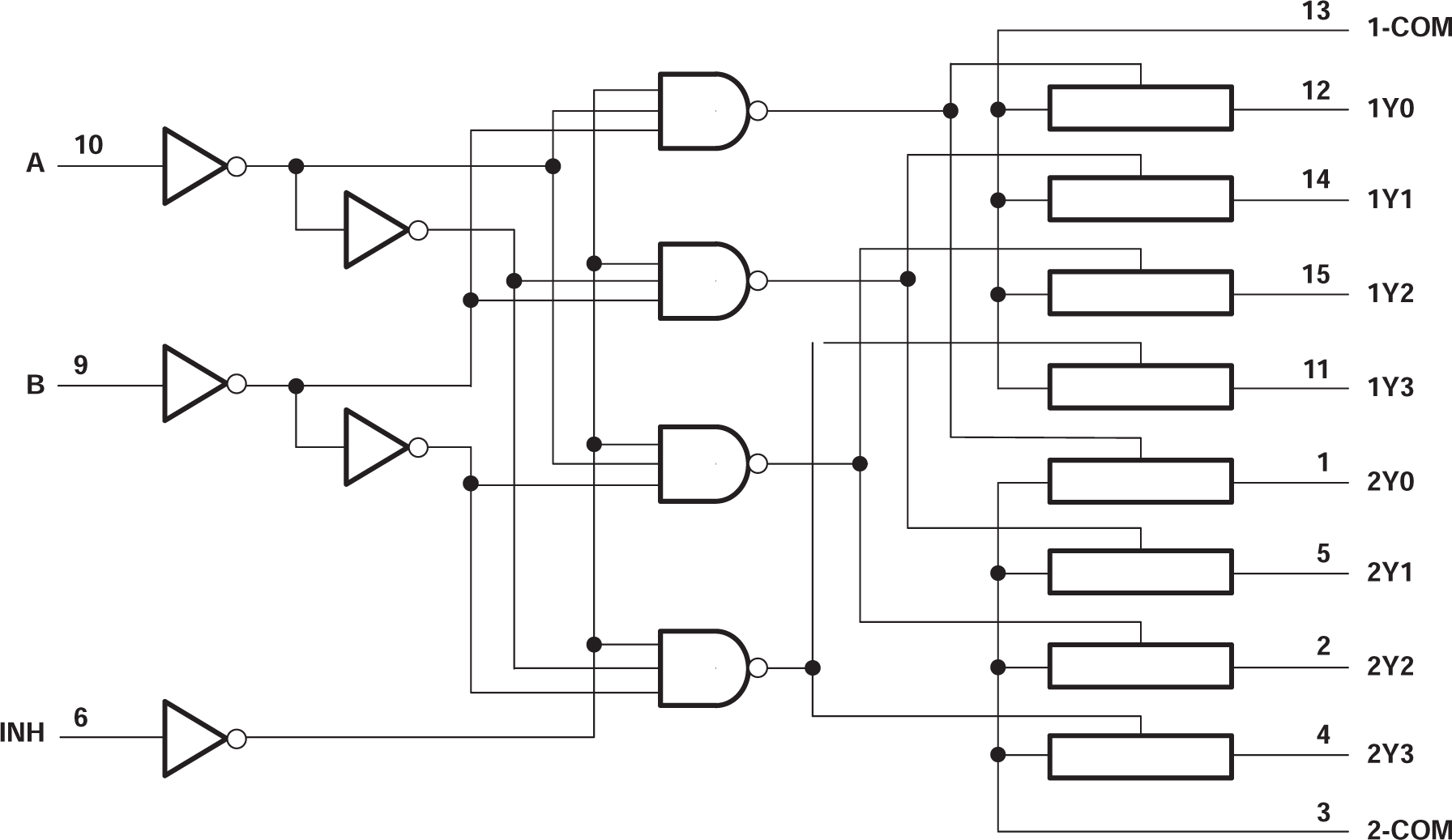
 Functional Diagram