SCLS600C November 2004 – June 2022 SN74HC573A-Q1
PRODUCTION DATA
- 1 Features
- 2 Description
- 3 Revision History
- 4 Pin Configuration and Functions
- 5 Specifications
- 6 Parameter Measurement Information
- 7 Detailed Description
- 8 Power Supply Recommendations
- 9 Layout
- 10Device and Documentation Support
- 11Mechanical, Packaging, and Orderable Information
Package Options
Refer to the PDF data sheet for device specific package drawings
Mechanical Data (Package|Pins)
- DW|20
- PW|20
Thermal pad, mechanical data (Package|Pins)
Orderable Information
2 Description
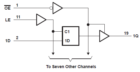
This octal transparent D-type latch features 3-state outputs designed specifically for driving highly capacitive or relatively low-impedance loads. It is particularly suitable for implementing buffer registers, I/O ports, bidirectional bus drivers, and working registers.
Device
Information
| PART NUMBER | PACKAGE(1) | BODY SIZE (NOM) |
|---|---|---|
| SN74HC573AQDW-Q1 | SOIC (20) | 12.80 mm × 7.50 mm |
| SN74HC573AQPW-Q1 | TSSOP (20) | 6.50 mm × 4.40 mm |
(1) For all
available packages, see the orderable addendum at
the end of the data sheet.
 Functional Block
Diagram