SCLS147G December 1982 – April 2022 SN54HC573A , SN74HC573A
PRODUCTION DATA
- 1 Features
- 2 Applications
- 3 Description
- 4 Revision History
- 5 Pin Configuration and Functions
- 6 Specifications
- 7 Parameter Measurement Information
- 8 Detailed Description
- 9 Application and Implementation
- 10Power Supply Recommendations
- 11Layout
- 12Device and Documentation Support
- 13Mechanical, Packaging, and Orderable Information
Package Options
Mechanical Data (Package|Pins)
Thermal pad, mechanical data (Package|Pins)
Orderable Information
3 Description
The SNx4HC573A devices are octal transparent
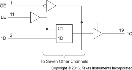
D-type latches that feature 3-state outputs designed specifically for driving highly capacitive or relatively low-impedance loads. They are particularly suitable for implementing buffer registers, I/O ports, bidirectional bus drivers, and working registers.
While the latch-enable (LE) input is high, the
Q outputs respond to the data (D) inputs. When LE is low, the outputs are latched to retain the data that was set up.
Device
Information(1)
| PART NUMBER | PACKAGE | BODY SIZE (NOM) |
|---|---|---|
| SN54HC573AJ | CDIP (20) | 26.92 mm × 6.92 mm |
| SN54HC573AW | CFP (20) | 13.72 mm × 6.92 mm |
| SN54HC573AFK | LCCC (20) | 8.89 mm × 8.89 mm |
| SN74HC573AN | PDIP (20) | 25.40 mm × 6.35 mm |
| SN74HC573ADW | SOIC (20) | 12.80 mm × 7.50 mm |
| SN74HC573ADB | SSOP (20) | 7.20 mm × 5.30 mm |
| SN74HC573APW | TSSOP (20) | 5.00 mm × 4.40 mm |
(1) For all available packages, see the orderable addendum at the end of the data sheet.
 Logic Diagram (Positive
Logic)