SCLS808C June 2020 – December 2021 SN74HCS164-Q1
PRODUCTION DATA
- 1 Features
- 2 Applications
- 3 Description
- 4 Revision History
- 5 Pin Configuration and Functions
- 6 Specifications
- 7 Parameter Measurement Information
- 8 Detailed Description
- 9 Application and Implementation
- 10Power Supply Recommendations
- 11Layout
- 12Device and Documentation Support
- 13Mechanical, Packaging, and Orderable Information
Package Options
Mechanical Data (Package|Pins)
Thermal pad, mechanical data (Package|Pins)
- BQA|14
Orderable Information
3 Description
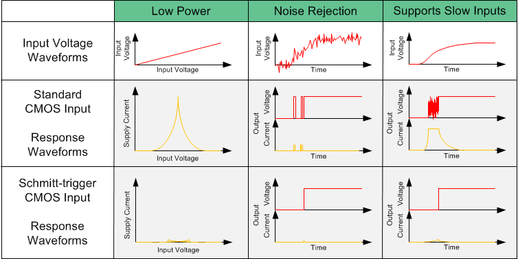
The SN74HCS164-Q1 device contains an 8-bit shift register with AND-gated serial inputs and an asynchronous clear (CLR) input. The gated serial (A and B) inputs permit complete control over incoming data; a low at either input inhibits entry of the new data and resets the first flip-flop to the low level at the next clock (CLK) pulse. A high-level input enables the other input, which then determines the state of the first flip-flop. Data at the serial inputs can be changed while CLK is high or low, provided the minimum set-up time requirements are met. Clocking occurs on the low-to-high-level transition of CLK. All inputs include Schmitt-triggers, eliminating any erroneous data outputs due to slow-edged or noisy input signals.
| PART NUMBER | PACKAGE(1) | BODY SIZE (NOM) |
|---|---|---|
| SN74HCS164PW-Q1 | TSSOP (14) | 5.00 mm × 4.40 mm |
| SN74HCS164D-Q1 | SOIC (14) | 8.65 mm × 3.91 mm |
| SN74HCS164BQA-Q1 | WQFN (14) | 3.00 mm × 2.50 mm |
| SN74HCS164DYY-Q1 | SOT-23-THIN (14) | 2.00 mm × 4.20 mm |
 Benefits of Schmitt-Trigger Inputs