SCLS872A November   2021  – February 2022 SN74HCS240-Q1

PRODUCTION DATA  

  1. Features
  2. Applications
  3. Description
  4. Revision History
  5. Pin Configuration and Functions
  6. Specifications
    1. 6.1 Absolute Maximum Ratings
    2. 6.2 ESD Ratings
    3. 6.3 Recommended Operating Conditions
    4. 6.4 Thermal Information
    5. 6.5 Electrical Characteristics
    6. 6.6 Switching Characteristics
    7. 6.7 Operating Characteristics
    8. 6.8 Typical Characteristics
  7. Parameter Measurement Information
  8. Detailed Description
    1. 8.1 Overview
    2. 8.2 Functional Block Diagram
    3. 8.3 Feature Description
      1. 8.3.1 Balanced CMOS 3-State Outputs
      2. 8.3.2 CMOS Schmitt-Trigger Inputs
      3. 8.3.3 Clamp Diode Structure
      4. 8.3.4 Wettable Flanks
    4. 8.4 Device Functional Modes
  9. Application and Implementation
    1. 9.1 Application Information
    2. 9.2 Typical Application
      1. 9.2.1 Design Requirements
        1. 9.2.1.1 Power Considerations
        2. 9.2.1.2 Input Considerations
        3. 9.2.1.3 Output Considerations
      2. 9.2.2 Detailed Design Procedure
      3. 9.2.3 Application Curve
  10. 10Power Supply Recommendations
  11. 11Layout
    1. 11.1 Layout Guidelines
    2. 11.2 Layout Example
  12. 12Device and Documentation Support
    1. 12.1 Documentation Support
      1. 12.1.1 Related Documentation
    2. 12.2 Receiving Notification of Documentation Updates
    3. 12.3 Support Resources
    4. 12.4 Trademarks
    5. 12.5 Electrostatic Discharge Caution
    6. 12.6 Glossary
  13. 13Mechanical, Packaging, and Orderable Information

Package Options

Mechanical Data (Package|Pins)
Thermal pad, mechanical data (Package|Pins)
Orderable Information

Clamp Diode Structure

The inputs and outputs to this device have both positive and negative clamping diodes as depicted in Figure 8-2.

CAUTION:

Voltages beyond the values specified in the Absolute Maximum Ratings table can cause damage to the device. The input and output voltage ratings may be exceeded if the input and output clamp-current ratings are observed.
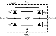
GUID-2FEC014A-6503-42D9-911A-C79AF74820AF-low.gif Figure 8-2 Electrical Placement of Clamping Diodes for Each Input and Output