SCLS807E june 2020 – july 2023 SN74HCS594-Q1
PRODUCTION DATA
- 1
- 1 Features
- 2 Applications
- 3 Description
- 4 Revision History
- 5 Pin Configuration and Functions
- 6 Specifications
- 7 Parameter Measurement Information
- 8 Detailed Description
- 9 Application and Implementation
- 10Power Supply Recommendations
- 11Layout
- 12Device and Documentation Support
- 13Mechanical, Packaging, and Orderable Information
Package Options
Mechanical Data (Package|Pins)
Thermal pad, mechanical data (Package|Pins)
- BQB|16
Orderable Information
3 Description
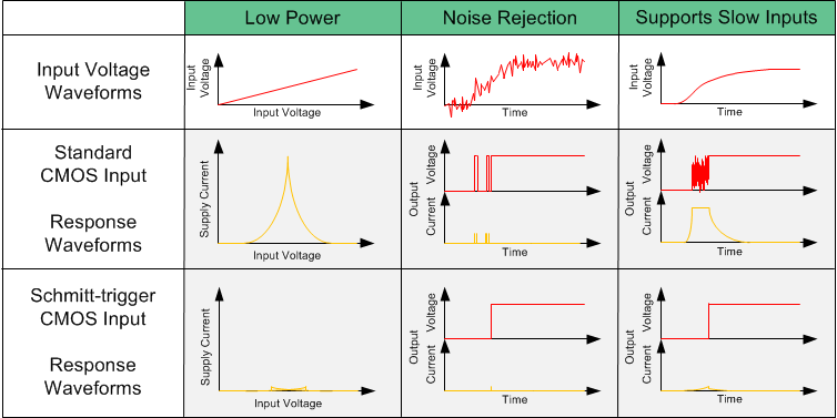
The SN74HCS594-Q1 device contains an 8-bit, serial-in, parallel-out shift register that feeds an 8-bit D-type storage register. All inputs include Schmitt-triggers, eliminating any erroneous data outputs due to slow-edged or noisy input signals. The storage register has parallel outputs. Separate clocks and direct overriding clear (SRCLR, RCLR) inputs are provided for both the shift and storage register. A serial output (QH') is provided for cascading.
Both the shift register (SRCLK) and storage register (RCLK) clocks are positive edge triggered. If both clocks are connected together, the shift register is one count pulse ahead of the storage register.
| PART NUMBER | PACKAGE(1) | PACKAGE SIZE(2) | BODY SIZE (NOM)(3) |
|---|---|---|---|
| SN74HCS594-Q1 | PW (TSSOP, 16) | 5 mm × 6.4 mm | 5 mm × 4.4 mm |
| D (SOIC, 16) | 9.9 mm × 6 mm | 9.9 mm × 3.9 mm | |
| BQB (WQFN, 16) | 3.5 mm × 2.5 mm | 3.5 mm × 2.5 mm | |
| DYY (SOT-23-THN, 16) | 4.2 mm × 2 mm | 4.2 mm × 2 mm | |
| WBQB (WQFN, 16) | 3.6 mm × 2.6 mm | 3.6 mm × 2.6 mm |
 Benefits of Schmitt-Trigger Inputs