SCLS788A
January 2020 – May 2020
SN74HCS7266
PRODUCTION DATA.
1
Features
2
Applications
3
Description
Device Images
Benefits of Schmitt-trigger Inputs
4
Revision History
5
Pin Configuration and Functions
Pin Functions
6
Specifications
6.1
Absolute Maximum Ratings
6.2
ESD Ratings
6.3
Recommended Operating Conditions
6.4
Thermal Information
6.5
Electrical Characteristics
6.6
Switching Characteristics
6.7
Typical Characteristics
7
Parameter Measurement Information
8
Detailed Description
8.1
Overview
8.2
Functional Block Diagram
8.3
Feature Description
8.3.1
Balanced CMOS Push-Pull Outputs
8.3.2
CMOS Schmitt-Trigger Inputs
8.3.3
Clamp Diode Structure
8.4
Device Functional Modes
9
Application and Implementation
9.1
Application Information
9.2
Typical Application
9.2.1
Design Requirements
9.2.1.1
Power Considerations
9.2.1.2
Input Considerations
9.2.1.3
Output Considerations
9.2.2
Detailed Design Procedure
9.2.3
Application Curves
10
Power Supply Recommendations
11
Layout
11.1
Layout Guidelines
11.2
Layout Example
12
Device and Documentation Support
12.1
Documentation Support
12.1.1
Related Documentation
12.2
Related Links
12.3
Community Resources
12.4
Trademarks
12.5
Electrostatic Discharge Caution
12.6
Glossary
13
Mechanical, Packaging, and Orderable Information
Package Options
Mechanical Data (Package|Pins)
PW|14
MPDS360A
D|14
MPDS177H
Thermal pad, mechanical data (Package|Pins)
Orderable Information
scls788a_oa
scls788a_pm
5
Pin Configuration and Functions
D or
PW Package
14-Pin
SOIC or
TSSOP
Top View
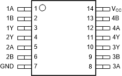
Pin Functions
PIN
I/O
DESCRIPTION
NAME
NO.
1A
1
Input
Channel 1, Input A
1B
2
Input
Channel 1, Input B
1Y
3
Output
Channel 1, Output Y
2Y
4
Output
Channel 2, Output Y
2A
5
Input
Channel 2, Input A
2B
6
Input
Channel 2, Input B
GND
7
—
Ground
3A
8
Input
Channel 3, Input A
3B
9
Input
Channel 3, Input B
3Y
10
Output
Channel 3, Output Y
4Y
11
Output
Channel 4, Output Y
4A
12
Input
Channel 4, Input A
4B
13
Input
Channel 4, Input B
V
CC
14
—
Positive Supply