SCES894E April 2019 – December 2021 SN74HCS74-Q1
PRODUCTION DATA
- 1 Features
- 2 Applications
- 3 Description
- 4 Revision History
- 5 Pin Configuration and Functions
- 6 Specifications
- 7 Parameter Measurement Information
- 8 Detailed Description
- 9 Application and Implementation
- 10Power Supply Recommendations
- 11Layout
- 12Device and Documentation Support
- 13Mechanical, Packaging, and Orderable Information
Package Options
Mechanical Data (Package|Pins)
Thermal pad, mechanical data (Package|Pins)
- BQA|14
Orderable Information
3 Description
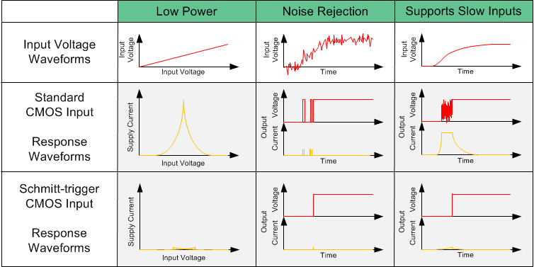
The device contains two independent D-type positive-edge-triggered flip-flops. All inputs include Schmitt triggers, allowing for slow or noisy input signals. A low level at the preset ( PRE) input sets the output high. A low level at the clear ( CLR) input resets the output low. Preset and clear functions are asynchronous and not dependent on the levels of the other inputs. When PRE and CLR are inactive (high), data at the data (D) input meeting the setup time requirements is transferred to the outputs (Q, Q) on the positive-going edge of the clock (CLK) pulse. Clock triggering occurs at a voltage level and is not directly related to the rise time of the input clock (CLK) signal. Following the hold-time interval, data at the data (D) input can be changed without affecting the levels at the outputs (Q, Q).
| PART NUMBER | PACKAGE(1) | BODY SIZE (NOM) |
|---|---|---|
| SN74HCS74PW-Q1 | TSSOP (14) | 5.00 mm × 4.40 mm |
| SN74HCS74D-Q1 | SOIC (14) | 8.70 mm × 3.90 mm |
| SN74HCS74BQA-Q1 | WQFN (14) | 3.00 mm × 2.50 mm |
| SN74HCS74DYY-Q1 | SOT-23-THIN (14) | 2.00 mm x 4.20 mm |
 Benefits of
Schmitt-trigger inputs