SCLS066E March 1982 – August 2022 SN74HCT139
PRODUCTION DATA
- 1 Features
- 2 Description
- 3 Revision History
- 4 Description (continued)
- 5 Pin Configuration and Functions
- 6 Specifications
- 7 Parameter Measurement Information
- 8 Detailed Description
- 9 Power Supply Recommendations
- 10Layout
- 11Device and Documentation Support
- 12Mechanical, Packaging, and Orderable Information
Package Options
Refer to the PDF data sheet for device specific package drawings
Mechanical Data (Package|Pins)
- DB|16
- PW|16
- N|16
- D|16
Thermal pad, mechanical data (Package|Pins)
Orderable Information
5 Pin Configuration and Functions
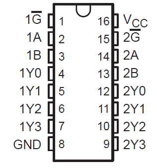
 Figure 5-1 SN54HCT139 J or W
Package
Figure 5-1 SN54HCT139 J or W
PackageSN74HCT139 D, DB, N, or PW Package
Top View

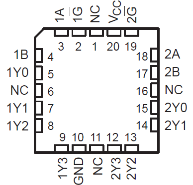
A. NC - No internal connection
Figure 5-2 SN54HCT139 FK PackageTop View