SCLS174H March 1984 – August 2024 SN54HCT240 , SN74HCT240
PRODUCTION DATA
- 1
- 1 Features
- 2 Description
- 3 Pin Configuration and Functions
- 4 Specifications
- 5 Parameter Measurement Information
- 6 Detailed Description
- 7 Application and Implementation
- 8 Device and Documentation Support
- 9 Revision History
- 10Mechanical, Packaging, and Orderable Information
Package Options
Refer to the PDF data sheet for device specific package drawings
Mechanical Data (Package|Pins)
- NS|20
- N|20
- DGS|20
- DW|20
- PW|20
Thermal pad, mechanical data (Package|Pins)
Orderable Information
2 Description
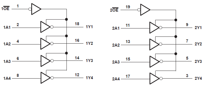
These octal buffers and line drivers are designed specifically to improve both the performance and density of 3-state memory address drivers, clock drivers, and bus-oriented receivers and transmitters. The ’HCT240 devices are organized as two 4-bit buffers/drivers with separate output-enable (OE) inputs. When OE is low, the device passes inverted data from the A inputs to the Y outputs. When OE is high, the outputs are in the high-impedance state.
| PART NUMBER | PACKAGE(1) | PACKAGE SIZE(2) | BODY SIZE(3) |
|---|---|---|---|
| SN74HCT240 | DGS (VSSOP, 20) | 5.1mm × 4.9mm | 5.1mm × 3mm |
| DW (SOIC, 20) | 12.80mm x 10.3mm | 12.80mm x 7.50mm | |
| PDIP (20) | 24.33mm × 9.4mm | 24.33mm × 6.35mm | |
| NS (SOP, 20) | 12.6mm x 7.8mm | 12.6mm x 5.3mm | |
| PW (TSSOP, 20) | 6.50mm x 6.4mm | 6.50mm x 4.40mm | |
| SN54HCT240 | J (CDIP, 20) | 24.2mm x 7.62mm | 24.2 mm x 6.92mm |
| FK (LCCC, 20) | 8.9mm x 8.9mm | 8.9mm x 8.9mm |
 Functional Block
Diagram