SDLS020F May 1990 – July 2016 SN54LS06 , SN74LS06
PRODUCTION DATA.
- 1 Features
- 2 Applications
- 3 Description
- 4 Revision History
- 5 Pin Configuration and Functions
- 6 Specifications
- 7 Parameter Measurement Information
- 8 Detailed Description
- 9 Application and Implementation
- 10Power Supply Recommendations
- 11Layout
- 12Device and Documentation Support
- 13Mechanical, Packaging, and Orderable Information
Package Options
Mechanical Data (Package|Pins)
Thermal pad, mechanical data (Package|Pins)
Orderable Information
1 Features
- Convert TTL Voltage Levels to MOS Levels
- High Sink-Current Capability
- Input Clamping Diodes Simplify System Design
- Open-Collector Driver for Indicator Lamps and Relays
- Inputs Fully Compatible With Most TTL Circuits
- On Products Compliant to MIL-PRF-38535, All Parameters Are Tested Unless Otherwise Noted. On All Other Products, Production Processing Does Not Necessarily Include Testing of All Parameters.
2 Applications
- Factory Automation
- Building Automation
- Line Drivers
- Electronic Point of Sale
- Desktop or Notebook PCs
3 Description
The SNx4LS06 devices feature high-voltage, open-collector outputs to interface with high-level circuits (such as MOS), or for driving high-current loads, and also are characterized for use as inverter buffers for driving TTL inputs. The SNx4LS06 devices have a rated output voltage of 30 V.
Device Information(1)
| PART NUMBER | PACKAGE | BODY SIZE (NOM) |
|---|---|---|
| SN54LS06 | CDIP (14) | 19.50 mm × 6.92 mm |
| LCCC (20) | 8.89 mm × 8.89 mm | |
| SN74LS06D | SOIC (14) | 8.65 mm × 3.91 mm |
| SN74LS06DB | SSOP (14) | 5.30 mm × 6.20 mm |
| SN74LS06N | PDIP (14) | 19.30 mm × 6.35 mm |
| SN74LS06NS | SOP (14) | 5.30 mm × 10.20 mm |
- For all available packages, see the orderable addendum at the end of the data sheet.
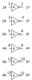
Logic Diagram (Positive Logic)

Pin numbers shown are for the D, DB, J, N, and NS packages.