SDLS153A January   1981  – January 2016 SN74LS292 , SN74LS294

PRODUCTION DATA.  

  1. Features
  2. Applications
  3. Description
  4. Revision History
  5. Pin Configuration and Functions
  6. Specifications
    1. 6.1 Absolute Maximum Ratings
    2. 6.2 Recommended Operating Conditions
    3. 6.3 Thermal Information
    4. 6.4 Electrical Characteristics
    5. 6.5 Switching Characteristics
    6. 6.6 Typical Characteristics
  7. Parameter Measurement Information
    1. 7.1 Logic Diagrams
  8. Detailed Description
    1. 8.1 Overview
    2. 8.2 Functional Block Diagram
    3. 8.3 Feature Description
    4. 8.4 Device Functional Modes
  9. Application and Implementation
    1. 9.1 Application Information
    2. 9.2 Typical Application
      1. 9.2.1 Design Requirements
      2. 9.2.2 Detailed Design Procedure
      3. 9.2.3 Application Curve
  10. 10Power Supply Recommendations
  11. 11Layout
    1. 11.1 Layout Guidelines
    2. 11.2 Layout Example
  12. 12Device and Documentation Support
    1. 12.1 Documentation Support
      1. 12.1.1 Related Documentation
    2. 12.2 Related Links
    3. 12.3 Community Resources
    4. 12.4 Trademarks
    5. 12.5 Electrostatic Discharge Caution
    6. 12.6 Glossary
  13. 13Mechanical, Packaging, and Orderable Information

Package Options

Mechanical Data (Package|Pins)
Thermal pad, mechanical data (Package|Pins)
Orderable Information

7 Parameter Measurement Information

7.1 Logic Diagrams
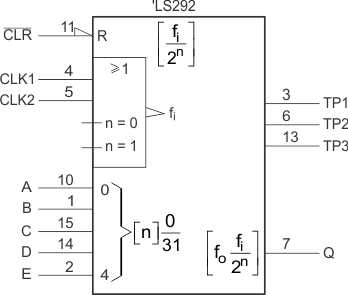
SN74LS292 SN74LS294 logic_symbol_01_SDLS153.gif
These symbols are in accordance with ANSi/IEEE Std 91-1984 and IEC Publication 617-12. Pin numbers shown are for J, N, and W packages.
Figure 4. Logic Symbols
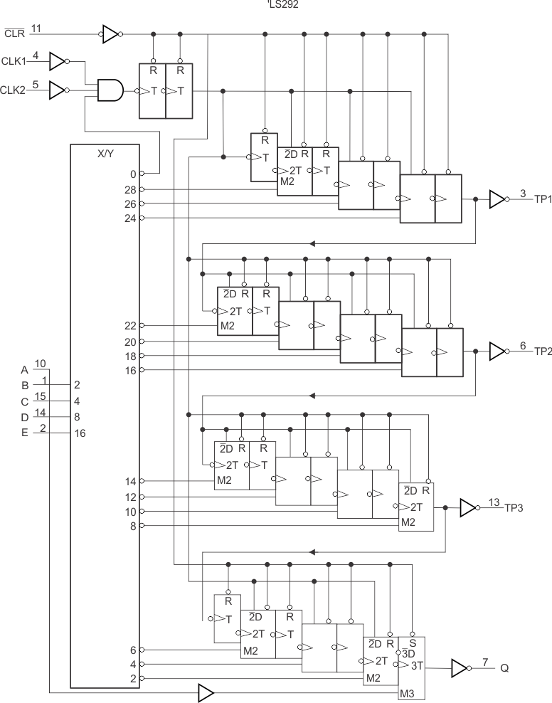
SN74LS292 SN74LS294 logic_symbol_03_SDLS153.gif
Pin numbers shown are for J, N, and W packages.
Figure 5. Logic Diagram (Positive Logic) SN74LS292
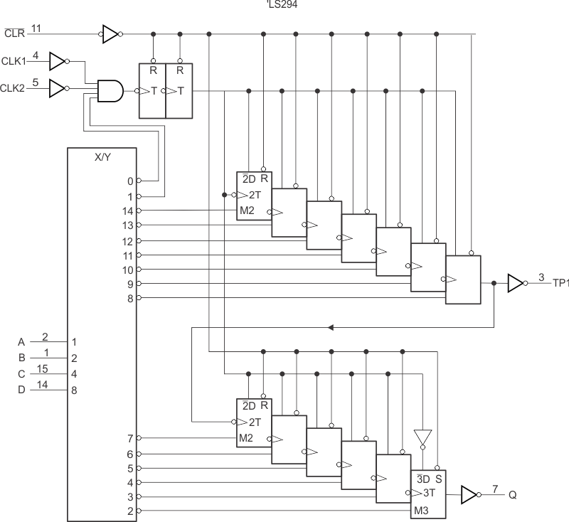
SN74LS292 SN74LS294 logic_symbol_04_SDLS153.gif
Pin numbers shown are for J, N, and W packages.
Figure 6. Logic Diagram (Positive Logic) SN74LS294