SCES468E july 2003 – july 2023 SN74LV11A-Q1
PRODMIX
- 1
- 1Features
- 2Description
- 3Revision History
- 4Pin Configuration and Functions
-
5Specifications
- 5.1 Absolute Maximum Ratings
- 5.2 ESD Ratings
- 5.3 Recommended Operating Conditions
- 5.4 Thermal Information
- 5.5 Electrical Characteristics
- 5.6 Switching Characteristics, VCC = 2.5 V ± 0.2 V
- 5.7 Switching Characteristics, VCC = 3.3 V ± 0.3 V
- 5.8 Switching Characteristics, VCC = 5 V ± 0.5 V
- 5.9 Noise Characteristics
- 5.10 Operating Characteristics
- 6Parameter Measurement Information
- 7Detailed Description
- 8Device and Documentation Support
- 9Mechanical, Packaging, and Orderable Information
Package Options
Mechanical Data (Package|Pins)
- PW|14
Thermal pad, mechanical data (Package|Pins)
Orderable Information
4 Pin Configuration and Functions
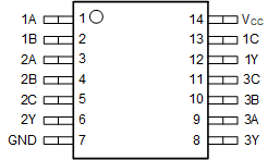
 Figure 4-1 SN74LV11A-Q1 PW Package (Top View)
| PIN | TYPE(1) | DESCRIPTION | |
|---|---|---|---|
| NAME | NO. | ||
| 1A | 1 | I | 1A Input |
| 1B | 2 | I | 1B Input |
| 2A | 3 | I | 2A Input |
| 2B | 4 | I | 2B Input |
| 2C | 5 | I | 2C Input |
| 2Y | 6 | O | 2Y Output |
| 3Y | 8 | O | 3Y Output |
| 3A | 9 | I | 3A Input |
| 3B | 10 | I | 3B Input |
| 3C | 11 | I | 3C Input |
| 1Y | 12 | O | 1Y Output |
| 1C | 13 | I | 1C Input |
| GND | 7 | — | Ground Pin |
| VCC | 14 | — | Power Pin |
(1) Signal Types: I = Input, O = Output.