SCES468E july 2003 – july 2023 SN74LV11A-Q1
PRODMIX
- 1
- 1Features
- 2Description
- 3Revision History
- 4Pin Configuration and Functions
-
5Specifications
- 5.1 Absolute Maximum Ratings
- 5.2 ESD Ratings
- 5.3 Recommended Operating Conditions
- 5.4 Thermal Information
- 5.5 Electrical Characteristics
- 5.6 Switching Characteristics, VCC = 2.5 V ± 0.2 V
- 5.7 Switching Characteristics, VCC = 3.3 V ± 0.3 V
- 5.8 Switching Characteristics, VCC = 5 V ± 0.5 V
- 5.9 Noise Characteristics
- 5.10 Operating Characteristics
- 6Parameter Measurement Information
- 7Detailed Description
- 8Device and Documentation Support
- 9Mechanical, Packaging, and Orderable Information
Package Options
Mechanical Data (Package|Pins)
- PW|14
Thermal pad, mechanical data (Package|Pins)
Orderable Information
2 Description
These triple 3-input positive-AND gates are designed for 2-V to 5.5-V VCC operation.
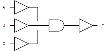
The SN74LV11A-Q1 devices perform the Boolean function Y = A • B • C or Y = A + B + C in positive logic.
These devices are fully specified for partial-power-down applications using Ioff. The Ioff circuitry disables the outputs, preventing damaging current backflow through the device when it is powered down.
 Simplified
Schematic