SCLS395N April 1998 – March 2023 SN74LV138A
PRODMIX
- 1 Features
- 2 Applications
- 3 Description
- 4 Revision History
- 5 Pin Configuration and Functions
-
6 Specifications
- 6.1 Absolute Maximum Ratings
- 6.2 ESD Ratings
- 6.3 Recommended Operating Conditions (1)
- 6.4 Thermal Information
- 6.5 Electrical Characteristics
- 6.6 Switching Characteristics, VCC = 2.5 V ± 0.25 V
- 6.7 Switching Characteristics, VCC = 3.3 V ± 0.3 V
- 6.8 Switching Characteristics, VCC = 5 V ± 0.5 V
- 6.9 Operating Characteristics
- 6.10 Typical Characteristics
- 7 Parameter Measurement Information
- 8 Detailed Description
- 9 Application and Implementation
- 10Device and Documentation Support
- 11Mechanical, Packaging, and Orderable Information
Package Options
Refer to the PDF data sheet for device specific package drawings
Mechanical Data (Package|Pins)
- BQB|16
- DB|16
- PW|16
- NS|16
- RGY|16
- D|16
- DGV|16
Thermal pad, mechanical data (Package|Pins)
Orderable Information
3 Description
The SN74LV138A device is 3-line to 8-line decoders/demultiplexers designed for 2 V to 5.5 V VCC operation.
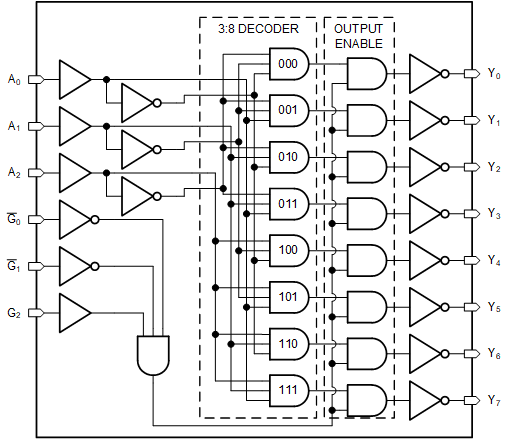
The conditions at the binary-select inputs (A0, A1, A2) and the three enable inputs (G2, G0, G1) select one of eight output lines. The two active-low (G0, G1) and one active-high (G2) enable inputs reduce the need for external gates or inverters when expanding.
Package Information
| PART NUMBER | PACKAGE(1) | BODY SIZE |
|---|---|---|
| SN74LV138A | D (SOIC, 16) | 9.90 mm × 3.91 mm |
| DB (SSOP, 16) | 6.20 mm × 5.30 mm | |
| DGV (TVSOP, 16) | 3.60 mm × 4.40 mm | |
| NSA (BGA, 16) | 2.00 mm × 2.00 mm | |
| PW (TSSOP, 16) | 5.00 mm × 4.40 mm | |
| RGY (VQFN, 16) | 4.00 mm × 3.50 mm | |
|
BQB (WQFN, 16) |
3.60 mm × 2.60 mm |
(1) For all available packages, see the orderable addendum at the end
of the data sheet.
 Logic Diagram (Positive Logic)