SCLS456D February 2001 – March 2023 SN74LV166A
PRODMIX
- 1 Features
- 2 Application
- 3 Description
- 4 Revision History
- 5 Pin Configuration and Functions
-
6 Specifications
- 6.1 Absolute Maximum Ratings
- 6.2 ESD Ratings
- 6.3 Recommended Operating Conditions
- 6.4 Thermal Information
- 6.5 Electrical Characteristics
- 6.6 Timing Requirements, VCC = 2.5 V ± 0.2 V
- 6.7 Timing Requirements, VCC = 3.3 V ± 0.3 V
- 6.8 Timing Requirements, VCC = 5 V ± 0.5 V
- 6.9 Switching Characteristics, VCC = 2.5 V ± 0.2 V
- 6.10 Switching Characteristics, VCC = 3.3 V ± 0.3 V
- 6.11 Switching Characteristics, VCC = 5 V ± 0.5 V
- Timing Diagram
- 6.12 Operating Characteristics
- 7 Parameter Measurement Information
- 8 Detailed Description
- 9 Application and Implementation
- 10Device and Documentation Support
- 11Mechanical, Packaging, and Orderable Information
Package Options
Refer to the PDF data sheet for device specific package drawings
Mechanical Data (Package|Pins)
- DB|16
- PW|16
- NS|16
- D|16
- DGV|16
Thermal pad, mechanical data (Package|Pins)
Orderable Information
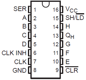
5 Pin Configuration and Functions
 D, DB, DGV, NS, or PW
Package
D, DB, DGV, NS, or PW
Package16-Pin SOP, SOIC, SSOP, TSSOP, TVSOP
(Top View)
Table 5-1 Pin Functions
| PIN | I/O | DESCRIPTION | |
|---|---|---|---|
| NAME | NO. | ||
| SER | 1 | I | Serial Output |
| A | 2 | I | Parallel Input |
| B | 3 | I | Parallel Input |
| C | 4 | I | Parallel Input |
| D | 5 | I | Parallel Input |
| CLK | 7 | I | Clock input |
| GND | 8 | __ | Ground |
| CLR | 9 | I | Clear input, active low |
| E | 10 | I | Parallel Input |
| F | 11 | I | Parallel Input |
| G | 12 | I | Parallel Input |
| QH | 13 | O | QH output |
| H | 14 | I | Parallel input H |
| SH/ LD | 15 | I | Shift/ load input, enable shifting when input is high, load data when input is low |
| VCC | 16 | __ | Power Pin |