SCLS738E September   2013  – May 2024 SN74LV1T04

PRODUCTION DATA  

  1.   1
  2. Features
  3. Applications
  4. Description
  5. Related Products
  6. Pin Configuration and Functions
  7. Specifications
    1. 6.1 Absolute Maximum Ratings
    2. 6.2 ESD Ratings
    3. 6.3 Recommended Operating Conditions
    4. 6.4 Thermal Information
    5. 6.5 Electrical Characteristics
    6. 6.6 Switching Characteristics
    7. 6.7 Operating Characteristics
    8. 6.8 Typical Characteristics
  8. Parameter Measurement Information
  9. Detailed Description
    1. 8.1 Overview
    2. 8.2 Functional Block Diagram
    3. 8.3 Feature Description
      1. 8.3.1 Clamp Diode Structure
      2. 8.3.2 Balanced CMOS Push-Pull Outputs
    4. 8.4 LVxT Enhanced Input Voltage
      1. 8.4.1 Down Translation
      2. 8.4.2 Up Translation
    5. 8.5 Device Functional Modes
  10. Application and Implementation
    1. 9.1 Power Supply Recommendations
    2. 9.2 Layout
      1. 9.2.1 Layout Guidelines
  11. 10Device and Documentation Support
    1. 10.1 Receiving Notification of Documentation Updates
    2. 10.2 Support Resources
    3. 10.3 Trademarks
    4. 10.4 Electrostatic Discharge Caution
    5. 10.5 Glossary
  12. 11Revision History
  13. 12Mechanical, Packaging, and Orderable Information

Package Options

Mechanical Data (Package|Pins)
Thermal pad, mechanical data (Package|Pins)
Orderable Information

Typical Characteristics

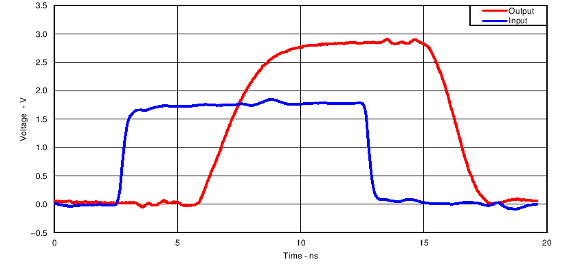
SN74LV1T04 Switching Characteristics at 50 MHz Excellent Signal Integrity  (1.8 V to 3.3 V at 3.3-V VCC)
Graph is from SN74LV1T34.
Figure 6-1 Switching Characteristics at 50 MHz
Excellent Signal Integrity
(1.8 V to 3.3 V at 3.3-V VCC)
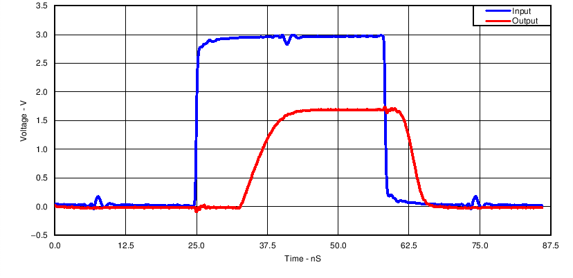
SN74LV1T04 Switching Characteristics at 15 MHz Excellent Signal Integrity (3.3 V to 1.8 V at 1.8-V VCC)
Graph is from SN74LV1T34.
Figure 6-3 Switching Characteristics at 15 MHz
Excellent Signal Integrity
(3.3 V to 1.8 V at 1.8-V VCC)
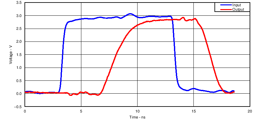
SN74LV1T04 Switching Characteristics at 50 MHz Excellent Signal Integrity (3.3 V to 3.3 V at 3.3-V VCC)
Graph is from SN74LV1T34.
Figure 6-2 Switching Characteristics at 50 MHz
Excellent Signal Integrity
(3.3 V to 3.3 V at 3.3-V VCC)