SCLS926A May 2023 – November 2023 SN74LV1T126-Q1
PRODUCTION DATA
- 1
- 1 Features
- 2 Applications
- 3 Description
- 4 Pin Configuration and Functions
-
5 Specifications
- 5.1 Absolute Maximum Ratings
- 5.2 ESD Ratings
- 5.3 Recommended Operating Conditions
- 5.4 Thermal Information
- 5.5 Electrical Characteristics
- 5.6 Switching Characteristics - 1.8-V VCC
- 5.7 Switching Characteristics - 2.5-V VCC
- 5.8 Switching Characteristics - 3.3-V VCC
- 5.9 Switching Characteristics - 5.0-V VCC
- 5.10 Typical Characteristics
- 6 Parameter Measurement Information
- 7 Detailed Description
- 8 Application and Implementation
- 9 Device and Documentation Support
- 10Revision History
- 11Mechanical, Packaging, and Orderable Information
Package Options
Refer to the PDF data sheet for device specific package drawings
Mechanical Data (Package|Pins)
- DBV|5
- DCK|5
Thermal pad, mechanical data (Package|Pins)
Orderable Information
3 Description
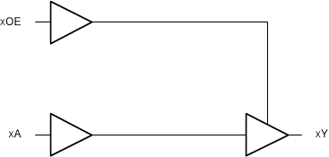
The SN74LV1T126-Q1 is a single buffer gate with 3-state outputs and integrated voltage translation. This buffer performs the Boolean function Y = A in positive logic. The outputs can be placed into a Hi-Z state by applying a Low on the OE pin. The output level is referenced to the supply voltage (VCC) and supports 1.8-V, 2.5-V, 3.3-V, and 5-V CMOS levels.
The input is designed with a lower threshold circuit to support up translation for lower voltage CMOS inputs (for example, 1.2 V input to 1.8 V output or 1.8 V input to 3.3 V output). In addition, the 5-V tolerant input pins enable down translation (for example, 3.3 V to 2.5 V output).
| PART NUMBER | PACKAGE(1) | PACKAGE SIZE(2) | BODY SIZE (NOM)(3) |
|---|---|---|---|
| SN74LV1T126-Q1 | DCK (SC70, 5) | 2 mm × 2.1 mm | 2 mm × 1.25 mm |
| DBV (SOT-23, 5) | 2.9 mm × 2.8 mm | 2.9 mm × 1.6 mm |
 Simplified Logic Diagram (Positive Logic)