SCLS383R september 1997 – august 2023 SN74LV244A
PRODMIX
- 1
- 1 Features
- 2 Applications
- 3 Description
- 4 Revision History
- 5 Pin Configuration and Functions
-
6 Specifications
- 6.1 Absolute Maximum Ratings
- 6.2 ESD Ratings
- 6.3 Recommended Operating Conditions
- 6.4 Thermal Information
- 6.5 Electrical Characteristics
- 6.6 Noise Characteristics
- 6.7 Operating Characteristics
- 6.8 Switching Characteristics: VCC = 2.5 V ± 0.2 V
- 6.9 Switching Characteristics: VCC = 3.3 V ± 0.3 V
- 6.10 Switching Characteristics: VCC = 5 V ± 0.5 V
- 6.11 Typical Characteristics
- 7 Parameter Measurement Information
- 8 Detailed Description
- 9 Application and Implementation
- 10Device and Documentation Support
- 11Mechanical, Packaging, and Orderable Information
5 Pin Configuration and Functions
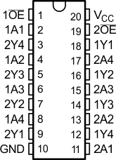
 Figure 5-1 DB, DGV, DW, NS, PW, or DGS Package, 20-Pin
SSOP, TVSOP, SOIC, SO, TSSOP, or VSSOP (Top View)
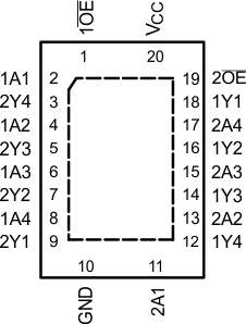
 Figure 5-2 RGY and RKS Package, 20-Pin VQFN With Exposed
Thermal Pad (Top View)
Figure 5-2 RGY and RKS Package, 20-Pin VQFN With Exposed
Thermal Pad (Top View)Table 5-1 Pin Functions
| PIN | TYPE(1) | DESCRIPTION | |
|---|---|---|---|
| NAME | NO. | ||
| 1A1 | 2 | I | Input |
| 1A2 | 4 | I | Input |
| 1A3 | 6 | I | Input |
| 1A4 | 8 | I | Input |
| 1 OE | 1 | I | Output enable |
| 1Y1 | 18 | O | Output |
| 1Y2 | 16 | O | Output |
| 1Y3 | 14 | O | Output |
| 1Y4 | 12 | O | Output |
| 2A1 | 11 | I | Input |
| 2A2 | 13 | I | Input |
| 2A3 | 15 | I | Input |
| 2A4 | 17 | I | Input |
| 2 OE | 19 | I | Output enable |
| 2Y1 | 9 | O | Output |
| 2Y2 | 7 | O | Output |
| 2Y3 | 5 | O | Output |
| 2Y4 | 3 | O | Output |
| GND | 10 | — | Ground |
| VCC | 20 | — | Power pin |
|
Thermal pad(2) |
— |
The thermal pad can be connected to GND or left floating. Do not connect to any other signal or supply. |
|
(1) Signal Types: I = Input, O = Output, I/O = Input or Output
(2) RKS package only