SCLS383R september 1997 – august 2023 SN74LV244A
PRODMIX
- 1
- 1 Features
- 2 Applications
- 3 Description
- 4 Revision History
- 5 Pin Configuration and Functions
-
6 Specifications
- 6.1 Absolute Maximum Ratings
- 6.2 ESD Ratings
- 6.3 Recommended Operating Conditions
- 6.4 Thermal Information
- 6.5 Electrical Characteristics
- 6.6 Noise Characteristics
- 6.7 Operating Characteristics
- 6.8 Switching Characteristics: VCC = 2.5 V ± 0.2 V
- 6.9 Switching Characteristics: VCC = 3.3 V ± 0.3 V
- 6.10 Switching Characteristics: VCC = 5 V ± 0.5 V
- 6.11 Typical Characteristics
- 7 Parameter Measurement Information
- 8 Detailed Description
- 9 Application and Implementation
- 10Device and Documentation Support
- 11Mechanical, Packaging, and Orderable Information
3 Description
The SN74LV244A octal buffers and line drivers are designed for 2-V to 5.5-V VCC operation.
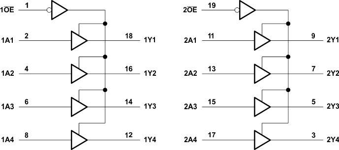
The SN74LV244A devices are designed specifically to improve both performance and density of the 3-state memory address drivers, clock drivers, and bus-oriented receivers and transmitters. These devices are organized as two 4-bit line drivers with separate output-enable (OE) inputs.
Package Information
| PART NUMBER | PACKAGE1 | PACKAGE SIZE2 |
|---|---|---|
| SN74LV244A | DB (SSOP, 20) | 7.2 mm × 7.8 mm |
| DGV (TVSOP, 20) | 5.00 mm × 6.4 mm | |
| DW (SOIC, 20) | 12.80 mm × 10.3 mm | |
| NS (SO, 20) | 12.60 mm × 5.30 mm | |
| PW (TSSOP, 20) | 6.50 mm × 7.8 mm | |
| RGY (VQFN, 20) | 4.5 mm × 3.50 mm | |
| RKS (VQFN, 20) | 4.50 mm × 2.50 mm | |
| DGS (VSSOP, 20) | 5.10 mm × 4.9 mm |
(1) For all available packages, see the orderable addendum at
the end of the data sheet.
(2) The package size (length × width)
is a nominal value and includes pins, where applicable.
 Logic Diagram (Positive Logic)