SCLS948 august 2023 SN74LV393B-EP
PRODUCTION DATA
- 1
- 1 Features
- 2 Applications
- 3 Description
- 4 Revision History
- 5 Pin Configuration and Functions
-
6 Specifications
- 6.1 Absolute Maximum Ratings
- 6.2 ESD Ratings
- 6.3 Recommended Operating Conditions
- 6.4 Thermal Information
- 6.5 Electrical Characteristics
- 6.6 Timing Requirements, VCC = 2.5 V ± 0.2 V
- 6.7 Timing Requirements, VCC = 3.3 V ± 0.3 V
- 6.8 Timing Requirements, VCC = 5 V ± 0.5 V
- 6.9 Switching Characteristics, VCC = 2.5 V ± 0.2 V
- 6.10 Switching Characteristics, VCC = 3.3 V ± 0.3 V
- 6.11 Switching Characteristics, VCC = 5 V ± 0.5 V
- 6.12 Noise Characteristics
- 6.13 Operating Characteristics
- 6.14 Typical Characteristics
- 7 Parameter Measurement Information
- 8 Detailed Description
- 9 Application and Implementation
- 10Device and Documentation Support
- 11Mechanical, Packaging, and Orderable Information
Package Options
Mechanical Data (Package|Pins)
- PW|14
Thermal pad, mechanical data (Package|Pins)
Orderable Information
3 Description
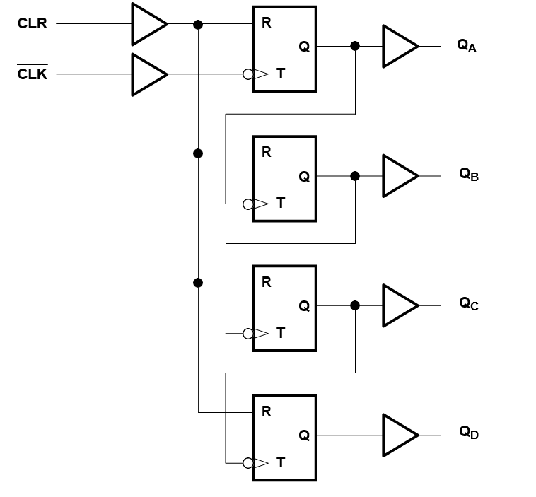
The SN74LV393B-EP contains eight flip-flops and additional gating to implement two individual 4-bit counters in a single package and is designed for 2 V to 5.5 V VCC operation.
This device fully specified for partial-power-down applications using Ioff. The Ioff circuitry disables the outputs, preventing damaging current backflow through the device when powered down.
(1) For all available packages, see the orderable addendum at the end of the data sheet.
(2) The package size (length × width) is a nominal value and includes pins, where
applicable.
 Logic Diagram (Positive Logic)