SCES656E February 2006 – November 2016 SN74LV4046A
PRODUCTION DATA.
- 1 Features
- 2 Applications
- 3 Description
- 4 Revision History
- 5 Pin Configuration and Functions
- 6 Specifications
- 7 Detailed Description
- 8 Application and Implementation
- 9 Power Supply Recommendations
- 10Layout
- 11Device and Documentation Support
- 12Mechanical, Packaging, and Orderable Information
Package Options
Mechanical Data (Package|Pins)
Thermal pad, mechanical data (Package|Pins)
Orderable Information
7 Detailed Description
7.1 Overview
The SN74LV4046A is a high-speed silicon-gate CMOS device that is pin compatible with the CD4046B and the CD74HC4046. The device is specified in compliance with JEDEC Std 7.
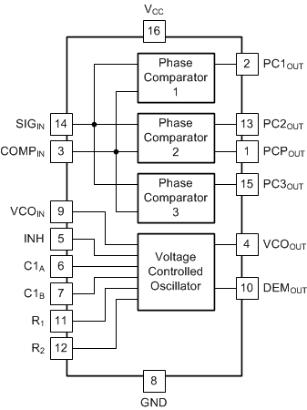
The SN74LV4046A is a phase-locked loop (PLL) circuit that contains a linear voltage-controlled oscillator (VCO) and three different phase comparators (PC1, PC2, and PC3) as explained in the Features section. A signal input and a comparator input are common to each comparator as shown in the Functional Block Diagram.
The signal input can be directly coupled to large voltage signals, or indirectly coupled (with a series capacitor) to small voltage signals. A self-bias input circuit keeps small voltage signals within the linear region of the input amplifiers. With a passive lowpass filter, the SN74LV4046A forms a second-order loop PLL. The excellent VCO linearity is achieved by the use of linear operational amplifier techniques. Various applications include telecommunications, Digital Phase Locked Loop and Signal generators.
The VCO requires one external capacitor C1 (between C1A and C1B) and one external resistor R1 (between R1 and GND) or two external resistors R1 and R2 (between R1 and GND, and R2 and GND). Resistor R1 and capacitor C1 determine the frequency range of the VCO. Resistor R2 enables the VCO to have a frequency offset if required. The high input impedance of the VCO simplifies the design of lowpass filters by giving the designer a wide choice of resistor or capacitor ranges. In order to not load the lowpass filter, a demodulator output of the VCO input voltage is provided at pin 10 (DEMOUT). In contrast to conventional techniques where the DEMOUT voltage is one threshold voltage lower than the VCO input voltage, here the DEMOUT voltage equals that of the VCO input. If DEMOUT is used, a load resistor (RS) should be connected from DEMOUT to GND; if unused, DEMOUT should be left open. The VCO output (VCOOUT) can be connected directly to the comparator input (COMPIN), or connected through a frequency divider. The VCO output signal has a specified duty factor of 50%. A LOW level at the inhibit input (INH) enables the VCO and demodulator, while a HIGH level turns both off to minimize standby power consumption.
7.2 Functional Block Diagram

7.3 Feature Description
There are three choices for the Phase Comparators in this device which are listed as follows:
- Phase comparator 1 (PC1) is an Exclusive OR network. The average output voltage from PC1, fed to VCO input through the low pass filter and seen at the demodulator output at pin 10 (VDEMOUT), is the resultant of the phase differences of signals (SIGIN) and the compartor input (COMPIN) as shown in Figure 7. The average of V DEM is equal to 1/2 VCC when there is no signal or noise at SIGIN, and with this input the VCO oscillates at the center frequency (fo).
- Phase comparator 2 (PC2) is an Edge-Triggered Flip-Flop. This is a positive edge-triggered phase and frequency detector. When the PLL is using this comparator, the loop is controlled by positive signal transitions and the duty factors of SIGIN and COMPIN are not important. PC2 comprises two D-type flip-flops, control-gating and a three-state output stage. The circuit functions as an up-down counter where SIGIN causes an up-count and COMPIN a down-count. The average output voltage from PC2, fed to the VCO through the lowpass filter and seen at the demodulator output at pin 10 (VDEMOUT), is the resultant of the phase differences of SIGIN and COMPINas in Figure 8.
- Phase comparator 3 (PC3) is an positive Edge-Triggered RS Flip-Flop. This is a positive edge-triggered sequential phase detector using an RS-type flip-flop. When the PLL is using this comparator, the loop is controlled by positive signal transitions and the duty factors of SIGIN and COMPIN are not important. The average output from PC3, fed to the VCO through the lowpass filter and seen at the demodulator at pin 10 (VDEMOUT), is the resultant of the phase differences of SIGIN and COMPIN as shown in Figure 9.
The excellent VCO linearity is achieved by the use of linear operational amplifier techniques. It has low standby power consumption using VCO inhibit control. Wide operating temperature range from –40°C to +125°C along with an optimized power supply voltage range from 3 V to 5.5 V.
7.4 Device Functional Modes
The SN74LV4046A device does not feature any special functional modes.