SCLS430M May 1999 – September 2024 SN74LV4053A
PRODUCTION DATA
- 1
- 1 Features
- 2 Applications
- 3 Description
- 4 Pin Configuration and Functions
-
5 Specifications
- 5.1 Absolute Maximum Ratings
- 5.2 ESD Ratings
- 5.3 Thermal Information: SN74LV4053A
- 5.4 Recommended Operating Conditions
- 5.5 Electrical Characteristics
- 5.6 Timing Characteristics VCC = 2.5 V ± 0.2 V
- 5.7 Timing Characteristics VCC = 3.3 V ± 0.3 V
- 5.8 Timing Characteristics VCC = 5 V ± 0.5 V
- 5.9 AC Characteristics
- 6 Parameter Measurement Information
- 7 Detailed Description
- 8 Application and Implementation
- 9 Device and Documentation Support
- 10Revision History
- 11Mechanical, Packaging, and Orderable Information
Package Options
Refer to the PDF data sheet for device specific package drawings
Mechanical Data (Package|Pins)
- DB|16
- PW|16
- DYY|16
- NS|16
- N|16
- RGY|16
- D|16
- DGV|16
Thermal pad, mechanical data (Package|Pins)
Orderable Information
3 Description
These triple 2-channel CMOS analog multiplexers/demultiplexers are designed for 1.65V to 5.5V VCC operation.
The SNx4LV4053A devices handle both analog and digital signals. Each channel permits signals with amplitudes up to 5.5V (peak) to be transmitted in either direction.
Applications include signal gating, chopping, modulation or demodulation (modem), and signal multiplexing for analog-to-digital and digital-to-analog conversion systems.
Package Information
| PART NUMBER | PACKAGE(1) | PACKAGE SIZE(2) |
|---|---|---|
| SNx4LV4053A | D (SOIC, 16) | 9.9mm × 6mm |
| PW (TSSOP, 16) | 5mm × 6.4mm | |
| RGY (VQFN, 16) | 4mm × 3.5mm | |
| DYY (SOT-23-THIN, 16) | 4.2mm x 3.26mm |
(1) For more information, see Section 11.
(2) The package size (length × width) is a nominal value and includes
pins, where applicable.
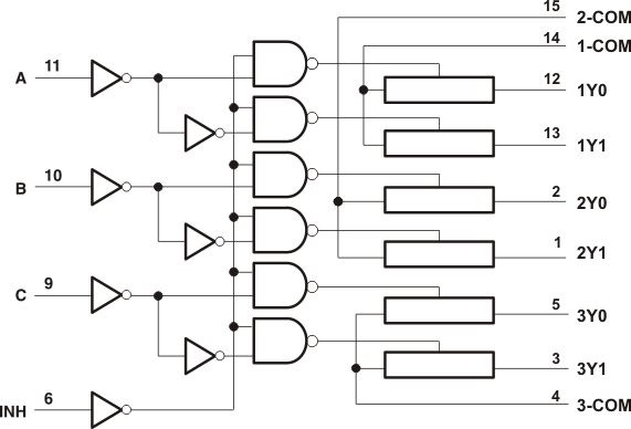
 Functional Block Diagram